The diode: Shockley equation, breakdown and models
The law of the junction, the diode equation with proof, characteristic and temperature, avalanche and Zener breakdown, capacitances and reverse recovery, Schottky, models and differential resistance.
The diode is the simplest semiconductor device: a pn junction with two contacts. It lets current through in one direction and blocks it in the other, but not like an ideal switch: its characteristic is exponential, depends on temperature and has capacitances that limit its speed. In this lesson we derive the diode equation and look at the models used in calculations.
The law of the junction
With a forward voltage  , the barrier drops from
 to
 . At the edges of the depletion region Boltzmann’s law still holds to a good approximation, and the concentration of injected minority carriers becomes

where 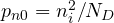 and
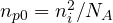 are the equilibrium values. A tenth of a volt is enough to multiply the minority carriers by
 .
The Shockley equation
Theorem. The current in an ideal diode is

Proof. On the n side, beyond the depletion region, the excess of injected holes  diffuses and recombines; as seen in the lesson on transport, it decays as
 . There is no field, so the current is pure diffusion, and at the edge

In the same way the electrons injected into the p side give  . Neglecting recombination in the thin depletion region, both currents cross it unchanged and the total current is their sum times the area
 . Substituting
 and
 gives the formula. ∎
The formula also shows that the current is carried mostly by the carriers of the more heavily doped side, injected into the more lightly doped one.
The characteristic
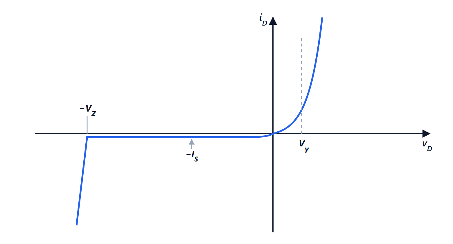
- Forward, the current grows by a factor of 10 every
 mV. With
 A: at 0.6 V 0.12 mA flows, at 0.65 V 0.82 mA, at 0.7 V 5.7 mA. That is why we speak of a threshold voltage
 of about 0.6 to 0.7 V for silicon: below it the current is negligible; above it small voltage changes give large current changes.
- Reverse, the current tends to
 , a few picoamperes or nanoamperes, in practice a little more because of generation in the depletion region.
Temperature.  is proportional to
 and roughly doubles every 5 °C. At constant current the forward voltage decreases by about 2 mV/°C: this is the principle of integrated temperature sensors, and the reason two diodes in parallel do not share current well (the one that heats up conducts more and heats up further).
Real diodes also have a series resistance (which makes the curve more linear at high currents) and an ideality factor  between 1 and 2 in the exponent,
 .
Breakdown
As the reverse voltage is increased, at some point the current rises sharply. There are two mechanisms:
- avalanche effect: in the strong field carriers gain enough energy to break bonds in collisions, and every pair created creates more. It dominates in lightly doped junctions, above 6 to 7 V;
- Zener effect: with very heavy doping the depletion region is so thin that electrons cross it by tunnelling. It dominates below about 5 V.
Breakdown is not destructive if the power is limited. Zener diodes are made specifically to work in that region: the voltage stays almost constant as the current changes and they serve as voltage references. The two mechanisms have opposite temperature coefficients, and around 5.6 V they cancel.
Capacitances and speed
- Junction capacitance, that of the depletion region (previous lesson): dominates in reverse.
- Diffusion capacitance: forward, a minority-carrier charge proportional to the current,
 , is stored in the neutral regions. To turn the diode off this charge must be removed, and for a short reverse recovery time the diode conducts backwards too. In the fast rectifiers of switching power supplies it is a major source of losses.
Schottky diodes, made with a metal-semiconductor junction, work with majority carriers only: they store no charge, are very fast and have a lower threshold, about 0.3 V.
Models for calculations
The exponential equation leads to nonlinear equations. Hand calculations use simpler models, chosen according to the accuracy needed:
| Model | Diode conducting | Typical use |
|---|---|---|
| ideal | short circuit, zero voltage | voltages much larger than 0.7 V |
| constant drop | 0.7 V source | almost all hand calculations |
| piecewise linear | 0.6 V in series with a small resistance | high currents |
| small signal | resistance 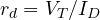 | small changes around the operating point |
The differential resistance. Differentiating the Shockley equation (with  ):
 , so
 . At 1 mA it is about 26 Ω, at 10 mA 2.6 Ω: for small changes the diode is a resistance that depends on the DC current through it. This is the first time we meet the idea of a small-signal model, the basis of every amplifier.