Power devices: conduction and switching losses, SiC and GaN
Diodes, MOSFETs, IGBTs and thyristors, conduction losses, switching energy proved with an example, gate driving and dead time, silicon carbide and gallium nitride.
Power electronics converts electrical energy from one form to another: from the AC mains to the DC of a charger, from an electric car’s battery to the three-phase voltage of the motor, from solar panels to the grid. It does so with electronic switches that open and close tens of thousands of times a second, because an ideal switch dissipates nothing: it has either zero voltage or zero current. Real switches, however, lose energy, and the efficiency, size and cost of every converter depend on these losses. In this lesson we look at power devices, conduction and switching losses with the proof of the energy lost in a transition and a numerical example, gate driving and wide-bandgap materials.
The devices
- Diodes: conduct in one direction only, without control. Power diodes have an important problem, reverse recovery: at turn-off they conduct backwards for a short time, until the stored charge is removed, causing losses and noise. Schottky diodes have no stored charge but withstand lower voltages.
- Power MOSFETs: voltage-controlled at the gate, very fast. When on they behave as a resistance
 , which however grows rapidly with the blocking voltage they are designed for: they are ideal up to a few hundred volts.
- IGBTs: combine MOSFET-type control with the conduction of a bipolar transistor. When on they have an almost constant drop, 1.5-2 V, advantageous at high currents and voltages (600-6500 V), but they turn off more slowly, with a current “tail”.
- Thyristors: turn on with a pulse and turn off only when the current falls to zero. Slow but extremely rugged, they are still used in controlled rectifiers and in ultra-high-voltage DC transmission (lesson on rectifiers).
Conduction losses
An on MOSFET carrying a current of RMS value  dissipates
 . An IGBT or a diode, with a roughly constant drop
 plus a small resistance, dissipate about
 . What matters, then, are the mean and RMS values of the current in the switch, which depend on the converter and on the duty cycle.
Switching losses
During the transition from off to on, and vice versa, voltage and current are simultaneously non-zero, and the switch dissipates. In the typical case, with an inductive load keeping the current constant at  and a supply voltage
 , at turn-on first the current rises at full voltage, then the voltage falls at full current.
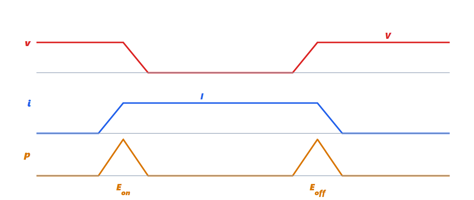
Theorem. If the current rises linearly in a time  at voltage and then the voltage falls linearly in a time
 at current , the energy lost at turn-on is
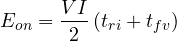
and the switching power loss, at frequency  , is
 .
Proof. In the first interval  and
 grows linearly from 0 to : the energy is
 . In the second
 and
 falls linearly from to 0: by symmetry the energy is
 . The sum gives
 ; turn-off is the same with the transitions in reverse order. Each period contains one turn-on and one turn-off, and there are periods per second. ∎
Example. A switch on a 400 V bus switching 10 A, with total transitions of 50 ns both at turn-on and at turn-off:  µJ. At 100 kHz the switching losses are
 W. A 50 mΩ MOSFET conducting half the time (
 A) instead dissipates only 2.5 W in conduction. Switching losses grow with frequency, and they are why frequency cannot be raised at will, even though higher frequencies would allow smaller inductors and capacitors (lesson on converters). With 5 ns transitions the losses would drop to 2 W.
Gate driving
A MOSFET’s gate is a capacitance: to turn it on it must be given a charge  , and the power spent by the driver is
 . The faster the gate is charged, the shorter the transitions and the lower the losses, but the faster the voltage and current changes, which generate electromagnetic interference (Electromagnetic Compatibility lessons). The gate driver must supply current peaks of a few amperes and, for switches whose source is not at ground, isolate the command.
In legs with two switches in series, as in inverter bridges (lesson on inverters), a dead time is inserted between turning one off and turning the other on, to prevent them from conducting together and short-circuiting the supply.
Wide-bandgap materials
Silicon is reaching its physical limits. Silicon carbide (SiC) and gallium nitride (GaN) have a bandgap about three times larger and a critical electric field about ten times larger: for the same blocking voltage the layer that must withstand it is much thinner and more heavily doped, and the on-resistance much lower. They switch faster, withstand higher temperatures and have negligible reverse recovery.
- SiC dominates between 650 and 1700 V: electric car inverters (where it has increased range by a few per cent), photovoltaics, fast chargers.
- GaN dominates below 650 V: phone and laptop chargers have become small thanks to switching frequencies of hundreds of kilohertz made possible by GaN.
The price is a cost still higher than silicon and transitions so fast that the printed circuit board layout, with its parasitic inductances, becomes critical.