DC-DC converters: volt-second balance, buck-boost and ripple
Volt-second and charge balance proved, the buck-boost ratio, current and voltage ripple proved with an example, discontinuous conduction, synchronous rectification, real limits.
The Applied Electronics course showed the buck and boost converters. Here we look at the method that makes it possible to analyse any switching converter in a few lines: the volt-second and charge balances in steady state, with proof. We apply it to the buck-boost converter, compute current and voltage ripple with proof, the boundary between continuous and discontinuous conduction, and look at synchronous rectification and the real limits of the conversion ratio.
The two steady-state principles
In steady state every quantity of the converter repeats identically in every switching period  .
Theorem. In periodic steady state:
- volt-second balance: the mean voltage across every inductor is zero,
 ;
- charge balance: the mean current in every capacitor is zero,
 .
Proof. For the inductor  . Integrating over one period:
 . In periodic steady state
 , so the integral, and with it the mean, is zero. For the capacitor, with
 , the same reasoning applies to the voltage. ∎
If the mean inductor voltage were not zero, the current would rise or fall a little every period: it would not yet be steady state. These two principles are enough to derive the conversion ratio of any converter.
The buck-boost converter
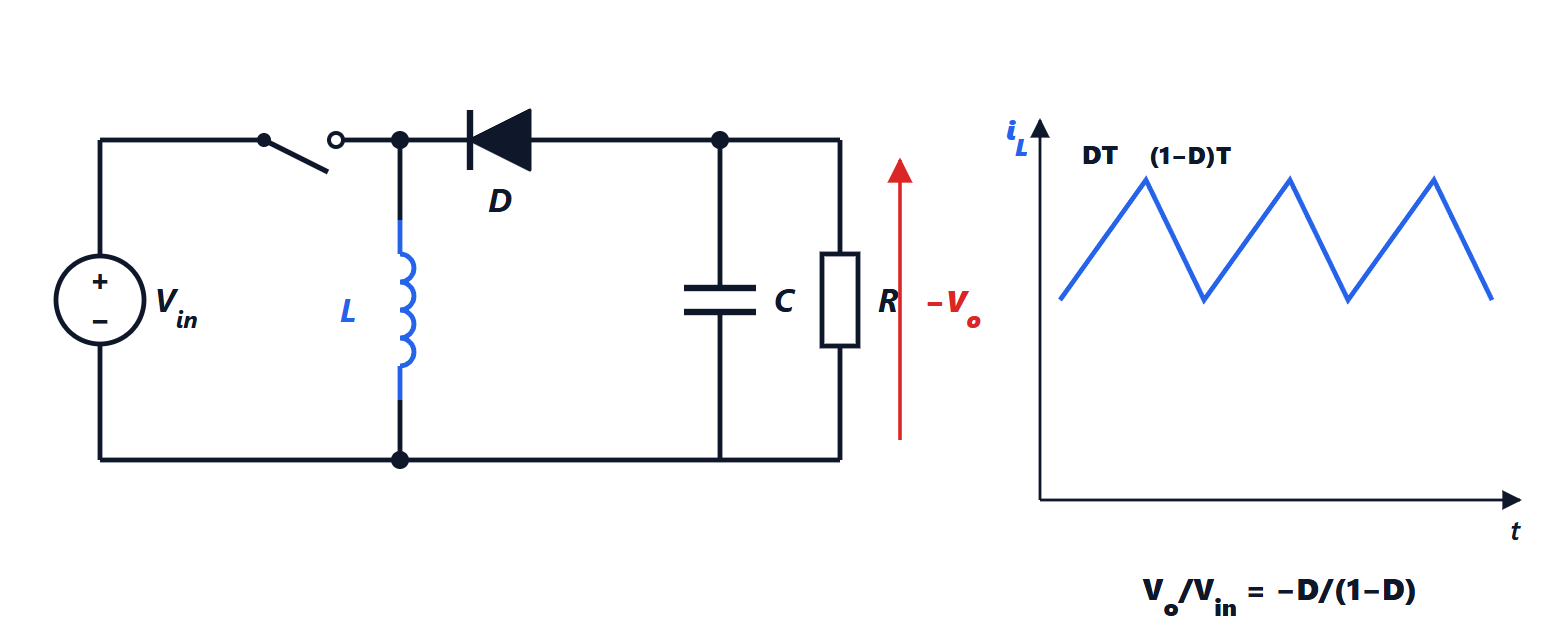
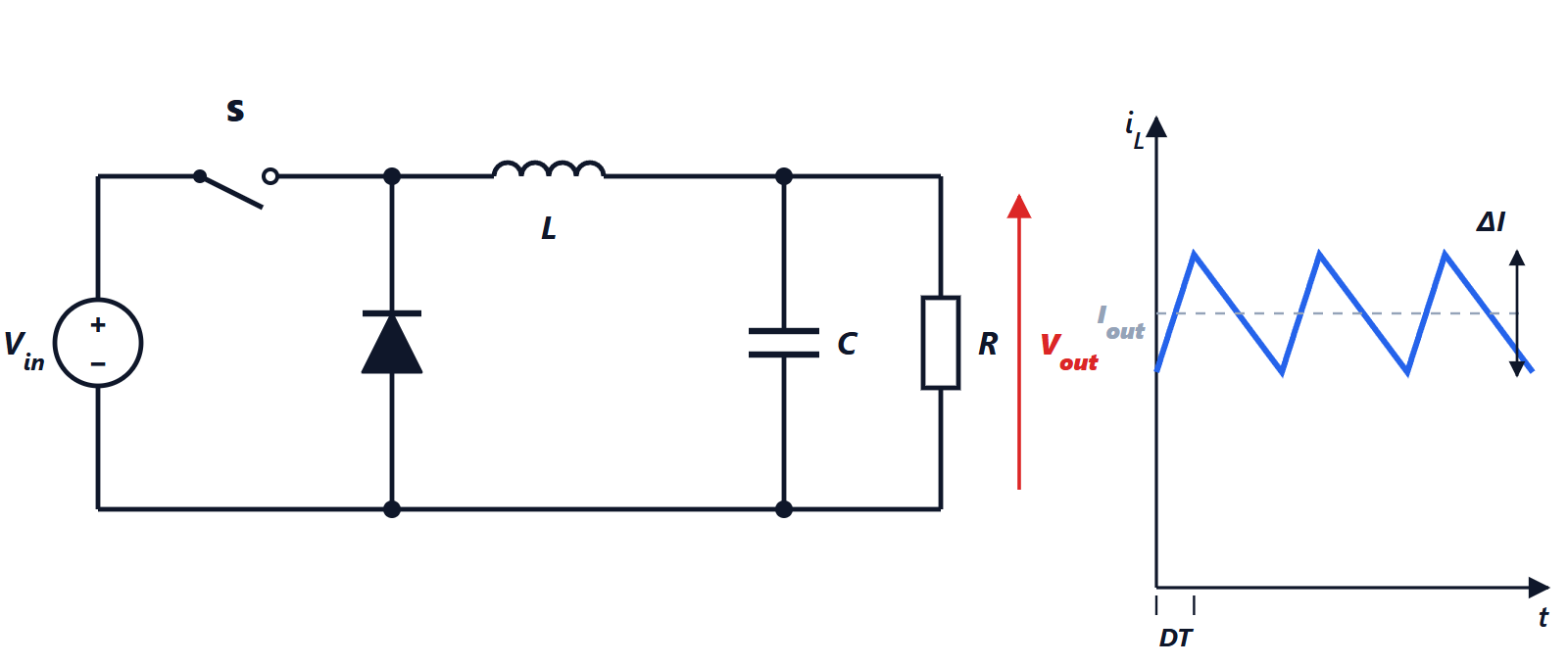
With the switch closed for a fraction  of the period (the duty cycle), the inductor is connected to the input:
 . With the switch open the inductor current flows through the diode to the output:
 , where
 is negative.
Theorem. In continuous conduction the conversion ratio of the buck-boost is
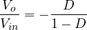
Proof. By volt-second balance  , which gives the formula. ∎
The magnitude of the output can be smaller than the input ( ) or larger (
 ), with reversed polarity. With the same method the buck (
 , so
 ) and the boost (
 ) are recovered in one line.
Ripple
Current. During the on-time the inductor current rises with slope  for a time
 : the peak-to-peak ripple is
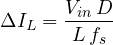
Doubling the frequency halves the inductance needed for the same ripple: this is the advantage of high frequencies, paid for with switching losses (lesson on devices).
Voltage. In the buck the inductor current goes to the capacitor and the load; the capacitor absorbs only the varying part, a triangular wave of peak-to-peak amplitude  .
Theorem. The peak-to-peak output voltage ripple of the buck is
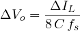
Proof. The capacitor current is positive for half a period, during which its shape is a triangle with base  and height
 . The accumulated charge is the area of the triangle,
 , and the voltage ripple is
 . ∎
Example. A buck from 12 to 3.3 V at 500 kHz with  µH:
 and, since in the buck the inductor sees
 during the on-time,
 A. With
 µF,
 mV. In practice the capacitor’s series resistance also matters, adding
 : that is why ceramic capacitors are used.
Continuous and discontinuous conduction
If the load draws little current, the minimum of the triangular wave drops to zero, and the diode prevents the current from becoming negative: for part of the period the inductor stays empty. This is discontinuous conduction (DCM), in which the conversion ratios derived above no longer hold and the output also depends on the load. The boundary is where the current minimum touches zero, i.e. where the mean inductor current equals . For the buck, with mean current equal to the load current  , the boundary gives a critical inductance
 . Converters at light load (in standby) often work in DCM or in burst mode on purpose, to reduce losses.
Synchronous rectification and real limits
The freewheeling diode has a 0.4-0.8 V drop: with a 1 V output, like the one supplying a processor, it would lose almost half the power. It is replaced by a second MOSFET driven in opposition to the first: synchronous rectification, with much lower  losses. The price is more complex driving with dead time.
The resistances of the inductor and the switches limit the real conversion ratio: in the boost the ideal formula  diverges as
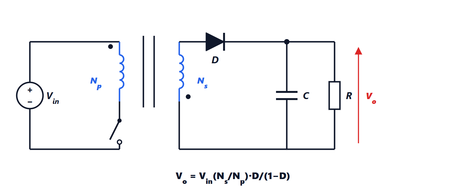
 , but in reality the output reaches a maximum and then collapses, because the input current becomes enormous and resistive drops dominate. That is why very high ratios are obtained with isolated converters with a transformer (dedicated lesson).