Power supplies: linear regulators and buck and boost converters
The linear regulator and its efficiency, LDOs, the buck converter with proven volt-second balance, current ripple with an example, the boost converter, interference and PFC.
Every electronic circuit needs stable DC voltages: 3.3 V for the microcontroller, 1 V for the processor, 5 V for USB, 12 V for a motor. They are derived from a battery or the mains with regulators, linear or switching. In this lesson we see how a linear regulator works and why it wastes energy, and how buck and boost switching converters achieve efficiencies above 90%.
The linear regulator
A transistor (the pass element) in series between input and output acts as a variable resistance; an error amplifier compares a fraction of the output with a stable reference voltage (a 1.2 V bandgap reference) and adjusts the transistor so that the output stays constant. It is a non-inverting feedback amplifier, with the reference as its input.
The flaw is efficiency. The load current flows through the transistor, which has the difference between input and output across it:

Example. From 12 V to 3.3 V at 1 A: the load receives 3.3 W and the regulator dissipates 8.7 W, an efficiency of 27.5%. A heat sink is needed, and a battery would last a quarter of what it could.
Linear regulators remain very valuable, though, when the difference is small or the current low: they are simple, cheap and above all quiet, with no switching noise. LDO (low dropout) regulators work with a difference between input and output of a few hundred millivolts, and are often used after a switching converter to clean up the supply of sensitive analogue circuits.
The buck converter
The buck (step-down) converter uses a switch, a diode (or a second switch), an inductor and a capacitor.
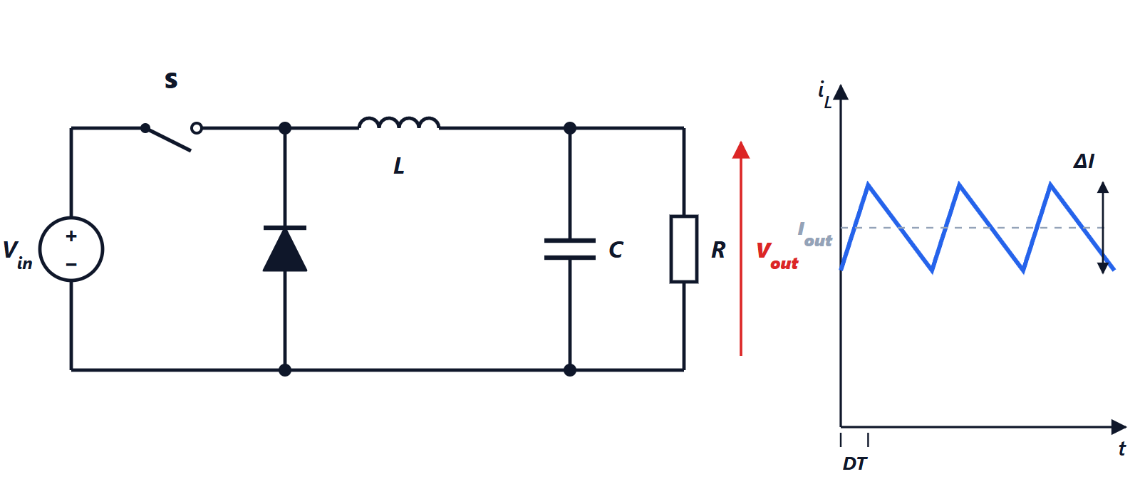
The switch closes for a fraction  of the period
 (the duty cycle) and opens for the rest. When it is closed, the inductor sits between
 and the output and its current rises; when it is open, the current keeps flowing through the diode and falls.
Theorem. In steady state and continuous conduction,

Proof. In steady state the inductor current at the start and end of each period is the same, so the average voltage across it is zero ( , integrated over a period, gives zero): this is the volt-second balance. During
 the voltage across the inductor is
 ; during
 , with the diode conducting,
 . So
 , that is
 . ∎
The converter is a DC transformer with an electronically adjustable ratio. Ideally it dissipates nothing: the switch has either zero voltage or zero current, the inductor and capacitor store energy without consuming it. Real converters reach 90 to 95%.
Current ripple. During the current rises by
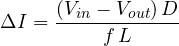
Example. From 12 V to 3.3 V:  . With
 kHz and
 µH,
 A. A higher frequency allows smaller inductors and capacitors, but increases switching losses: modern converters run between a few hundred kilohertz and a few megahertz, and with gallium nitride transistors even higher.
The boost converter
Swapping the positions of switch and inductor gives the boost (step-up) converter. With the switch closed the inductor charges from the input; when open, its voltage adds to the input voltage and pushes current to the output through the diode. The same volt-second balance ( ) gives
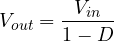
From 5 V to 12 V needs  . It is the converter that raises the voltage of a lithium cell (3.7 V) to the 5 V of a USB port in power banks, and the one that drives backlight LEDs.
In practice
Switching converters are everywhere, but they must be designed carefully: fast switching produces electromagnetic interference, contained with current loops kept as short as possible on the printed circuit board, ceramic capacitors close to the components and input filters. Finally, the pulsed currents of the rectifier feeding them from the mains cause the low power factor of power supplies, corrected with a PFC stage (Electrical Engineering lesson on power): that stage is itself a boost converter.