Solved transistor exercises: biasing, small-signal amplifiers and logic gates
Twelve exercises with solutions: divider design, pnp, sensitivity to beta, JFET and MOSFET, common emitter with degeneration, follower, common source, Miller effect and cascode, bypass capacitor, TTL and RTL fan-out.
Transistor exercises of the kind found in electronics exams, at three levels: basic, with the calculation of the operating point (npn and pnp BJT, JFET, MOSFET); intermediate, with small-signal amplifiers; exam, with frequency response and logic gates. Unless stated otherwise  V and
 mV are used. The result is given straight away; the complete step-by-step solution opens with a click. The proofs of the formulas are in the lessons on biasing, on small-signal amplifiers and on BJT logic gates.
Basic level
Exercise 1. Designing a divider bias
An npn BJT with  between 80 and 300 (mean value 150) must work with
 mA, a 15 V supply, 1.5 V on the emitter and 9 V on the collector. Size
 ,
 ,
 and
 with the rule
 , choose standard values and check the current with = 80, 150 and 300.
Result:  kΩ,
 kΩ,
 kΩ,
 kΩ;
 = 0.966, 1.016 and 1.047 mA.
Solution
1. From the desired voltages:  kΩ and
 kΩ (standard values: 5.6 or 6.2 kΩ; 6 kΩ is kept here to follow the calculations).
2. Stability rule:  kΩ. The Thévenin voltage must provide the drop across ,
 and the drop of the base current across
 (computed with the mean ):
 V.
3. From the divider:  kΩ and
 kΩ. Choosing 82 kΩ and 15 kΩ gives
 V and
 kΩ.
4. Check with  : with
 , 0.966 mA (
 V); with 150, 1.016 mA (7.37 V); with 300, 1.047 mA (7.14 V). A change of almost four times in moves the current by 8 %.
Exercise 2. A pnp
A pnp with  is powered from 9 V. The emitter goes to the supply through
 kΩ, the collector to ground through
 kΩ; the base is on a divider with 10 kΩ towards the supply and 33 kΩ towards ground. Find , the emitter and collector voltages and
 .
Result:  mA,
 V,
 V,
 V.
Solution
1. With a pnp it is convenient to measure voltages downwards from the supply. The divider brings the base  V below the supply, with
 kΩ.
2. The loop supply, , emitter-base junction, gives the same formula as the npn:  mA, and
 mA.
3. The emitter sits  V below the supply: V. The collector sits
 V above ground.
 V: the transistor is in the active region, with a wide margin.
Exercise 3. Sensitivity to beta
In the divider circuit of the lesson ( kΩ,
 kΩ,
 ) compute the relative sensitivity of the current to and use it to estimate the change in current when goes from 200 to 220. Compare with the exact calculation.
Result:  ; estimate +0.51 %, exact value +0.47 %.
Solution
1.  Ω, and
 .
2. A 10 % increase in (about 10 % in  too) produces a relative change in the current of
 %.
3. The exact calculation, with for 200 and 220, gives +0.47 %. The first-order estimate is slightly pessimistic because the sensitivity decreases as grows. With fixed bias the current would rise by 10 %.
Exercise 4. Self-biased JFET
An n-channel JFET with  mA and
 V must work at
 mA with self-bias. Find
 ,
 and the transconductance. What current is obtained with the same by fitting a unit with
 mA and
 V?
Result:  V,
 Ω,
 mS; with the other unit 2.77 mA.
Solution
1. From Shockley’s law:  , hence
 V.
2. With self-bias  :
 Ω.
3. Differentiating Shockley’s law:  mS (which is also
 ).
4. With the other unit one solves  , looking for the root with between −4 V and 0:
 mA. The current changes by 39 % for a 50 % change in
 : self-bias helps little.
Exercise 5. MOSFET with drain feedback
An n-channel MOSFET with  mA/V² and
 V has a 1 MΩ resistor between drain and gate and
 kΩ to the 10 V supply; the source is grounded. Find ,
 and
 , and check that the transistor is in saturation.
Result:  V,
 mA,
 mS.
Solution
1. No current flows in the gate:  .
2. Letting  :
 (with in mA and ), that is,
 , whose positive root is
 V. Hence
 V and
 mA.
3.  mS.
4. Saturation:  V >
 V. As proved in the lesson, with this connection it is always true.
Intermediate level
Exercise 6. Common emitter with and without degeneration
A common-emitter stage has mA, ,  kΩ and load
 kΩ. Compute the voltage gain and the input resistance seen from the base with the emitter fully bypassed, and then with 220 Ω unbypassed.
Result: bypassed:  ,
 kΩ; with 220 Ω:
 ,
 kΩ.
Solution
1.  mS,
 kΩ,
 kΩ.
2. Bypassed emitter:  ,
 kΩ.
3. With  Ω:
 ; the approximate formula
 is almost identical.
 kΩ.
4. Degeneration divides the gain by about 10, multiplies the input resistance by 10 and makes the gain independent of (and therefore of current and temperature):  if
 is neglected too.
Exercise 7. The follower as an impedance converter
A source with an internal resistance of 10 kΩ must drive a 100 Ω load. Compute the signal reaching the load when connected directly, and through an emitter follower with  ,
 mA and
 kΩ (ignore the bias divider). Also find the output resistance of the follower.
Result: directly 0.99 %; with the follower 46.7 %;  Ω.
Solution
1. Direct connection:  . The signal arrives reduced a hundredfold.
2. Follower:  Ω; on the emitter
 Ω.
 kΩ and
 .
3. With the source:  . The signal on the load is 47 times larger than with the direct connection.
4.  Ω: the source resistance, seen from the load, is divided by .
Exercise 8. Common source
A MOSFET with  mA/V² works at
 mA, with
 kΩ and a 20 kΩ load. Compute , the overdrive voltage and the gain with the source bypassed and with 500 Ω unbypassed. Compare with a BJT at the same current.
Result:  mS,
 V;
 and
 ; the BJT would have
 mS and
 .
Solution
1.  mS
 mS;
 V.
2.  kΩ. Bypassed:
 . With
 Ω:
 .
3. A BJT at 1 mA has  mS, fourteen times more, and . The ratio between the transconductances is
 : at the same current the BJT always wins, the MOSFET wins on input resistance and linearity.
Exam level
Exercise 9. The Miller effect
A common-emitter stage has  pF,
 pF, a base-to-collector gain of
 and an equivalent source resistance seen from the base of 1 kΩ. Estimate the upper cut-off frequency with the Miller approximation, and compare it with that of a cascode stage, in which the gain at the collector of the input transistor is about −1.
Result:  pF,
 MHz; with the cascode
 pF and about 6.1 MHz.
Solution
1. Miller’s theorem brings  to the input multiplied by
 : 303 pF. With
 , pF.
2. The input pole:  MHz.
3. In the cascode the collector of the input transistor is connected to the emitter of a common-base transistor, which has resistance : the base-to-collector gain is about −1, and is multiplied only by 2. The input capacitance becomes  pF and the bandwidth
 MHz: twelve times more, with the same overall gain. A 3 pF capacitance, the smallest in the transistor, alone decides the bandwidth of the common-emitter stage.
Exercise 10. The bypass capacitor
In a common-emitter stage with kΩ fully bypassed,  kΩ, , and a source resistance in parallel with the divider of 900 Ω, what must
 be for its pole to be at 20 Hz?
Result: resistance seen 32.6 Ω;  µF (270 µF is chosen).
Solution
1. The capacitor sees in parallel with the resistance looking into the transistor’s emitter:  Ω. In parallel with 1 kΩ: 32.6 Ω.
2.  µF; the next standard value is 270 µF.
3. Coupling capacitors see resistances of kΩ and a few µF are enough; the bypass capacitor sees a few tens of ohms and must be a hundred times larger. This is why part of is often left unbypassed: it raises the resistance seen and reduces .
Exercise 11. Fan-out between TTL families
A standard 74 TTL output ( mA,
 µA) drives 74LS inputs (
 mA,
 µA). How many can it drive? And how many standard 74 inputs (
 mA,
 µA) can a 74LS output (
 mA, µA) drive?
Result: 20 in the first case; 5 in the second.
Solution
1. The fan-out is the minimum of the low-level and the high-level fan-outs. 74 → 74LS:  at the low level and
 at the high level: 20.
2. 74LS → 74:  at the low level,
 at the high level: 5. The limit is the current flowing out of the low standard inputs, which the LS output must sink.
3. Mixing families is possible because the voltage levels are compatible, but the fan-out must be recomputed with the currents of each.
Exercise 12. RTL fan-out
An RTL gate has  V,
 Ω,
 Ω and
 V. How many gates can it drive if the high level must not fall below 1 V?
Result:  : at most 7 gates.
Solution
1. From the formula of the lesson,  V.
2. Isolating  :
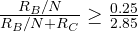 , that is,
 , and
 .
3. With 7 loads  V, with 8 it drops to 0.98 V. Even with 7 loads the margin above the conduction threshold (0.75 V) is only 0.25 V: this is why RTL was replaced by DTL and TTL.


Ciao, sono l'autore di «Esercizi sui transistor svolti: polarizzazione, amplificatori per piccolo segnale e porte logiche». Domande, dubbi, segnalazioni di errori o richieste di approfondimento sono benvenuti: scriveteli qui sotto e vi rispondo io. Potete anche votare la pagina con le stelle all'inizio dell'articolo.Hi, I am the author of “Solved transistor exercises: biasing, small-signal amplifiers and logic gates”. Questions, doubts, error reports and requests for more detail are all welcome: write them below and I will answer. You can also rate the page with the stars at the top of the article.