The MOSFET: threshold, channel equation and operating regions
Structure, the MOS capacitor and inversion, the triode equation with proof, saturation and the square law, operating regions, second-order effects, pMOS and power MOSFETs.
The MOSFET (metal-oxide-semiconductor field-effect transistor) is the most manufactured device in human history: a modern processor contains tens of billions of them. It works very differently from the BJT: current flows in a thin channel near the surface, and the gate voltage controls it through an insulator, drawing no DC current. In this lesson we derive its equations.
The structure
In a p-type substrate (body, B) there are two heavily doped n⁺ regions, the source (S) and the drain (D). Between them, on top of the surface, lies a very thin insulating layer (silicon oxide, or higher-permittivity materials) and above that the gate electrode (G). The distance between source and drain is the channel length  , the dimension perpendicular to the drawing is the width
 .
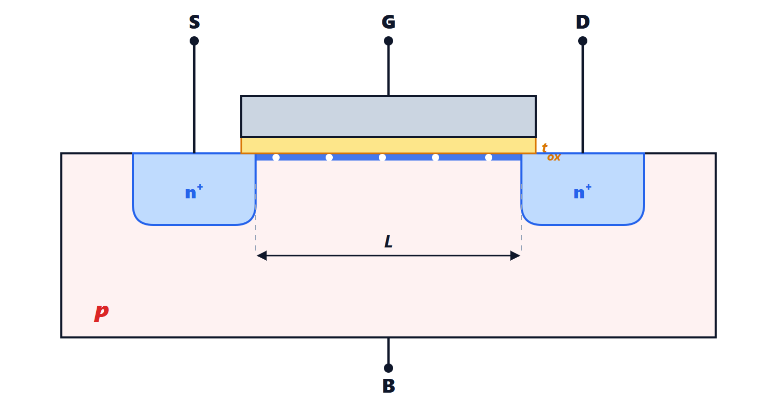
With no gate voltage, between source and drain there are two back-to-back pn junctions: whatever the sign of  , one of them is reverse biased and no current flows.
The MOS capacitor and the threshold
Gate, oxide and substrate form a capacitor with capacitance per unit area  . With
 nm,
 µF/cm².
Applying a positive voltage to the gate:
- the substrate holes are pushed away from the surface, leaving a depletion region with the negative acceptor ions;
- as the voltage increases, the surface also attracts electrons (minority carriers in p-type), which gather in a very thin layer under the oxide;
- beyond the threshold voltage
 the surface electrons outnumber the substrate holes: the surface has inverted to n-type, and this layer connects source and drain. It is the channel.
Beyond threshold, every extra volt on the gate adds a charge per unit area  to the channel: gate and channel are the two plates of the capacitor. In current processes is between about 0.2 and 0.5 V.
The MOSFET equation
Theorem. For  and
 (the triode region), the drain current is

Proof (gradual channel approximation). Let  be the channel potential at point
 , from 0 at the source to at the drain. At that point the effective gate-to-channel voltage is
 , and the electron charge per unit area is

The current is drift along the channel and is the same through every cross-section:  (charge times width times velocity, with velocity
 ). Separating variables and integrating from source to drain:


which is the formula. ∎
Saturation
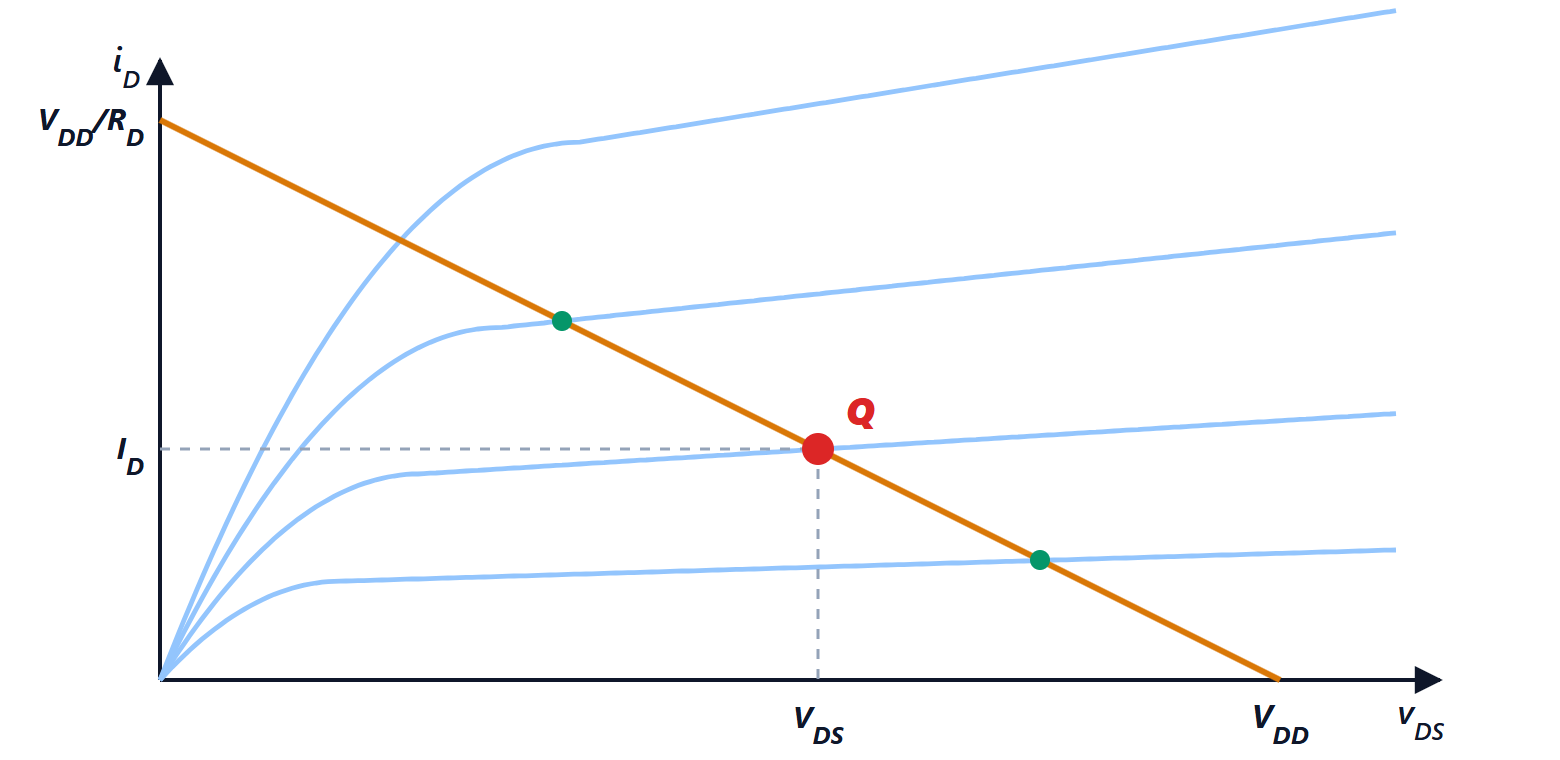
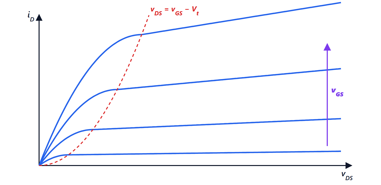
The triode formula is a parabola in with its maximum at  . At that point the channel charge at the drain vanishes: the channel is pinched off. Increasing further, the pinch-off point moves only slightly towards the source and the extra voltage drops across the short depleted stretch near the drain, which electrons cross pushed by the field. The current stays at the maximum value:

This is the square law. The quantity  is called the overdrive voltage, and
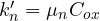 is the process parameter.
Example.  mA/V²,
 V,
 V: in saturation
 mA. With a very small , instead, the quadratic term is negligible and the transistor is a gate-controlled resistance:
 kΩ.
Operating regions
| Region | Condition | Current | Use |
|---|---|---|---|
| cut-off |  | almost zero | open switch |
| triode | | triode formula | closed switch, variable resistance |
| saturation |  | square law | amplifier, current source |
Mind the name: MOSFET “saturation” corresponds to the BJT active region, not to BJT saturation.
Second-order effects
- Channel length modulation. In saturation the pinch-off point moves and the effective channel gets a little shorter:
 grows slightly with , as in the Early effect, written
 . The output resistance is
 .
- Body effect. If the source is not at the substrate potential, the threshold increases.
- Subthreshold conduction. Below the current is not zero but drops exponentially, at best by a factor of 10 every 60 mV. This is why the threshold cannot be lowered as much as one would like: billions of “off” transistors would leak too much current.
- Short channel. In modern transistors, with of a few tens of nanometres, the velocity saturates and the square law becomes almost linear in
 .
Variants
- The pMOS has an n substrate, p⁺ source and drain and a hole channel: voltages and currents have opposite sign and, for the same size, it conducts about half as much because of the lower hole mobility.
- Depletion-mode MOSFETs have a channel already present at
 and a negative threshold.
- Power MOSFETs have vertical structures with thousands of cells in parallel and an on-resistance
 of a few milliohms: they switch tens of amperes in power supplies and motor drives.
The insulated gate is the MOSFET’s great advantage: at DC it draws no current, so driving it costs only the charge of the gate capacitance. It is also its weak point: the oxide is extremely thin, and an electrostatic discharge punches through it. That is why integrated circuits have the protection diodes seen in the lesson on diode circuits.