Differential amplifiers: bipolar and MOS pairs, degeneration, active load and cascode
Differential and common mode, gain and CMRR, large-signal characteristic with proof, the MOS pair, degeneration, active load, telescopic, folded cascode, fully differential and offset.
Inside every operational amplifier, at the input, there is a differential amplifier: two identical transistors that amplify the difference between two voltages and reject what they have in common. There are many variants, differing in transistor type, linearity, gain and signal swing. In this lesson we analyse the bipolar and MOS differential pair, including large signals, degeneration, the different kinds of load (resistive, active, cascode), the telescopic, folded cascode and fully differential configurations, and the offset due to mismatch.
Differential mode and common mode
Two input voltages  and
 can always be written as

the differential signal and the common-mode signal, with  and
 . The useful signal is almost always in the difference; the common mode is a disturbance: 50 Hz hum picked up equally by both wires of a cable, the DC voltage of a measurement bridge, differences between the grounds of two instruments.
The differential pair with resistive load
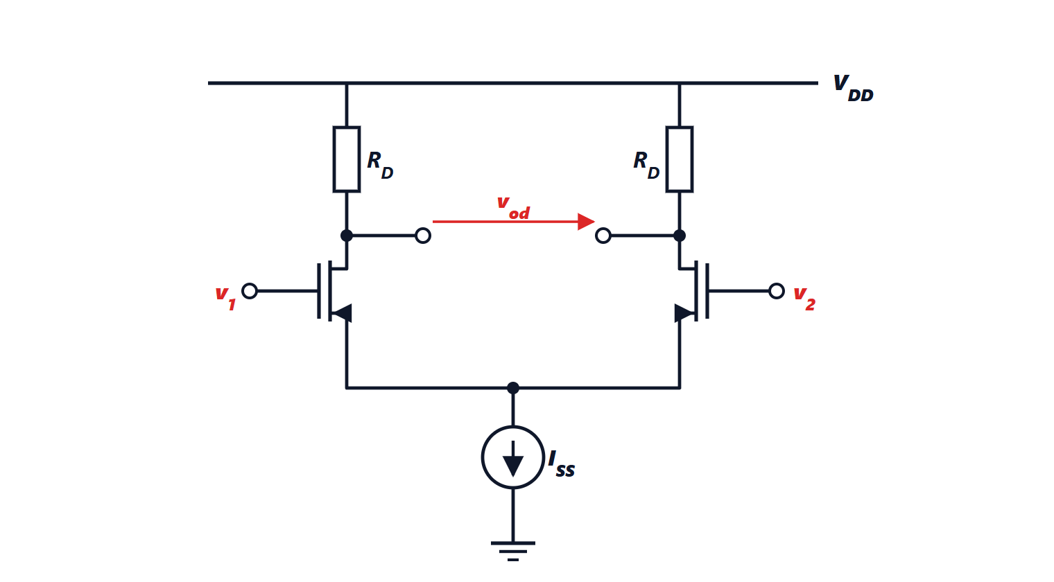
Two identical transistors with their sources (or emitters) tied together to a tail current source. The sum of the two currents is fixed: a difference between the inputs shifts current from one branch to the other, and the two outputs move in opposite directions.
Theorem (small-signal differential gain). The differential output between the two drains is

with  the transconductance of each transistor at half the tail current.
Proof. With a purely differential input,  on one gate and
 on the other, by symmetry the current in one branch increases by exactly as much as the other decreases; the common source node does not change voltage and is, for small signals, a virtual ground. Each half is a common-source amplifier:
 ,
 . The difference is
 . ∎
With the output taken from one drain the gain is halved. For the common mode, a real tail source with output resistance  gives a gain (at one output) of
 , and quality is measured by the CMRR
 : with
 and
 , 100 dB.
Large-signal behaviour
Theorem (bipolar pair). With tail current  , the difference between the collector currents is

Proof. The emitters are at the same potential, so  . With
 (neglecting base currents) we get
 ,
 , and the difference is
 . ∎
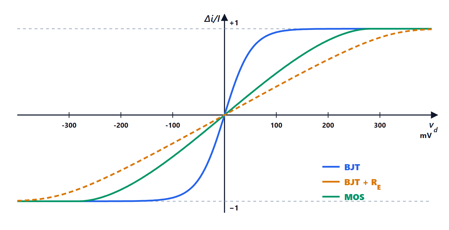
The bipolar pair is linear (within 1%) only for  about 9 mV, and beyond ±76 mV it has already moved 90% of the current to one side: it is an excellent current switch (it is the heart of ECL logic and of analogue multipliers, such as the Gilbert cell in radio mixers), but a linear amplifier only for very small signals.
The MOS pair. With the square law, 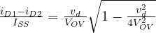 , and all the current goes to one side at
 . Increasing the overdrive voltage (narrower transistors or more current) widens the linear range, but lowers
 : a trade-off between linearity and gain.
Degeneration
Inserting a resistor  (or
 ) in series with each emitter, the effective transconductance becomes
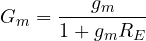
Example. A bipolar pair with 1 mA of tail current (0.5 mA per side,  mA/V),
 kΩ: without degeneration the gain is about 190; with
 Ω,
 and the gain drops to about 18, but the linear range widens by the same factor and the gain depends little on the transistor. It is the local feedback seen in the lesson on amplifiers.
The active load
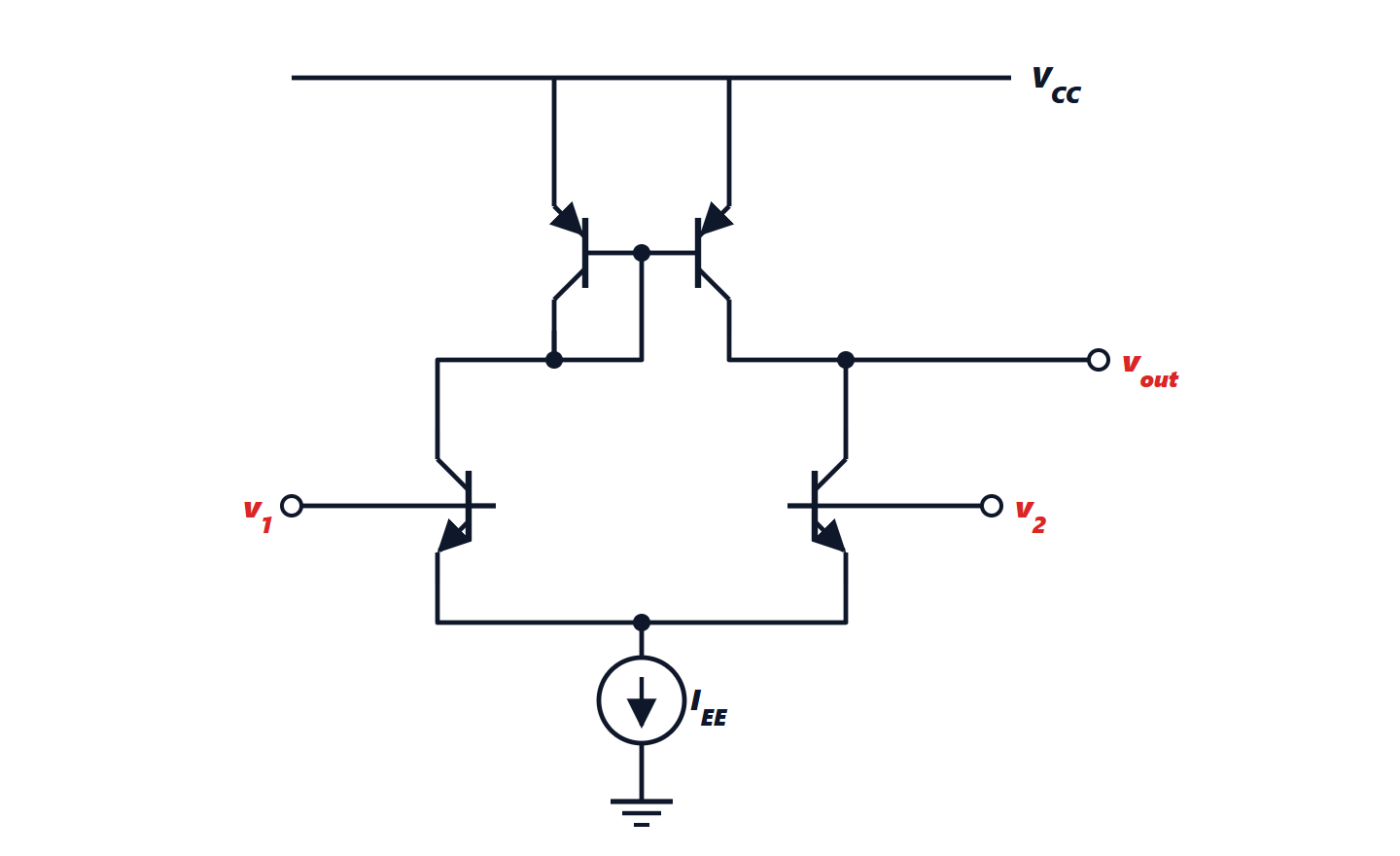
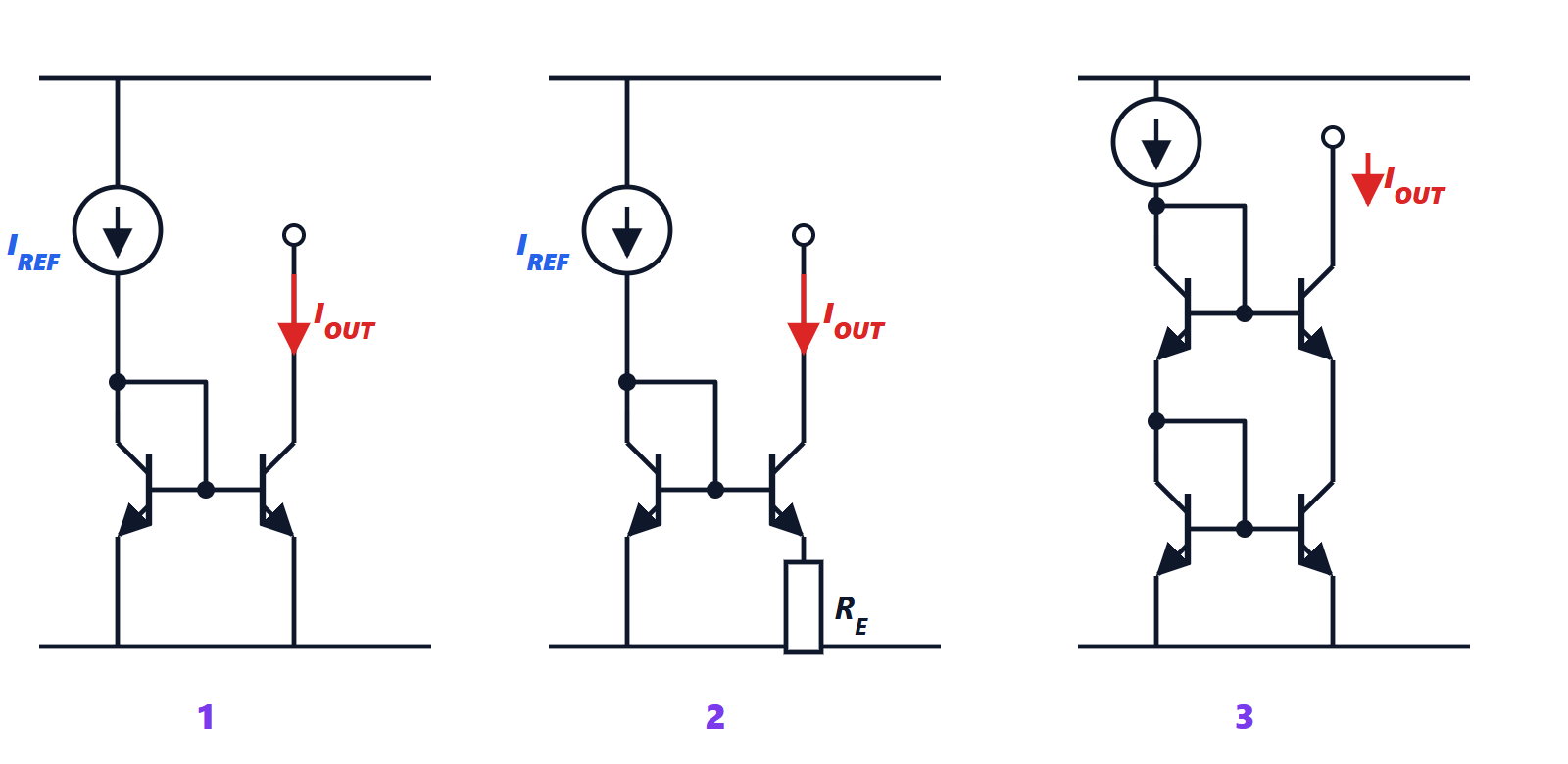
With a current mirror (next lesson) in place of the resistors, the left branch current is copied into the right branch. For a differential signal the left branch carries  and the right
 ; the copy of arrives at the output node and leaves it, so a net current
 flows in. This current flows through the parallel combination of the output resistances of the pair transistor and the mirror transistor:

Example. A bipolar pair with 0.5 mA per side and a 100 V Early voltage:  kΩ, the parallel is 100 kΩ and the gain is about
 in a single stage, with a single-ended output and without losing half of the signal. With short-channel MOSFETs (
 mA/V,
 kΩ) one gets about 50.
Cascode, telescopic and folded cascode
Higher gain requires higher output resistance. A common-gate transistor (cascode) on top of each pair transistor multiplies the output resistance by about  , and the same is done with the load mirror: this is the telescopic amplifier, with gain of the order of
 , thousands even with short MOSFETs, and excellent frequency response. The price is swing: four transistors stacked between the supplies leave little room for the signal, a serious problem with 1 to 1.8 V supplies.
The folded cascode solves the problem: the input pair current is “folded” into cascode transistors of the opposite type, connected to the other supply. Input and output swing improve a lot (with a pMOS input pair the common mode can reach ground), at the cost of a little more power and noise. It is the structure of very many integrated op-amps.
The fully differential amplifier
In high-performance integrated circuits (converters, filters, radio interfaces) the output is differential too: two outputs in antiphase, with twice the swing for the same supply and excellent rejection of common disturbances (supply, substrate). An extra circuit is needed, however, the common-mode feedback (CMFB), which measures the average of the two outputs and holds it at the desired value: differential feedback controls the difference but says nothing about the average, which would otherwise drift until it saturates.
Offset
Two “identical” transistors never quite are. In the bipolar pair a relative difference  between the saturation currents produces an offset voltage
 : with 1% mismatch, about 0.26 mV. In MOSFETs the difference between threshold voltages weighs most, a few millivolts, decreasing with transistor area. Designers reduce offset by laying out the pair with common-centroid geometries (each transistor split into interleaved parts, so that process gradients cancel) and, in the most demanding cases, with trimming or chopper techniques.
Inside an op-amp
A classic two-stage op-amp is made of a differential pair with active load (input, first gain, common-mode rejection), a common-emitter or common-source gain stage with the compensation capacitor that creates the dominant pole, and a class AB output stage. All the current sources biasing these stages are current mirrors fed from a single reference.