Current mirrors in depth: Early effect, Wilson, cascode and Widlar proved
Error due to the Early effect and base currents, helper transistor, Wilson and cascode mirrors with output resistances proved, wide-swing cascode, Widlar mirror solved by iteration, MOS mirrors with lambda.
This page goes deeper into the lesson on current mirrors: it derives step by step the formulas that the lesson only states, namely the error of the mirror with a helper transistor and of the Wilson mirror, the output resistance of the Wilson mirror and of the cascode with the small-signal model, the Early effect on the copy ratio, and shows how to solve the Widlar mirror equation, which has no closed-form solution. The quantities are those of the lesson:  current gain,
 mV at 300 K,
 Early voltage,
 ,
 .
The simple mirror with the Early effect
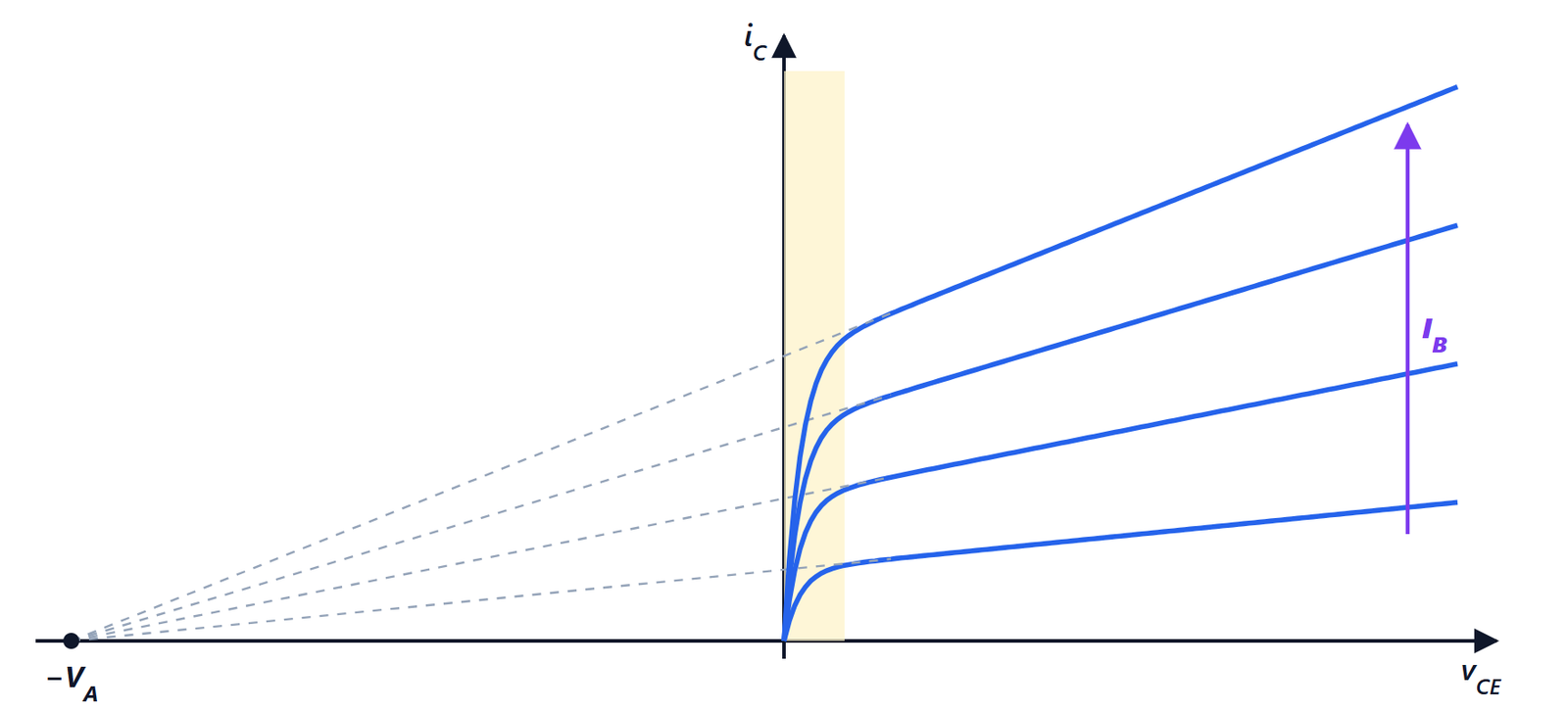
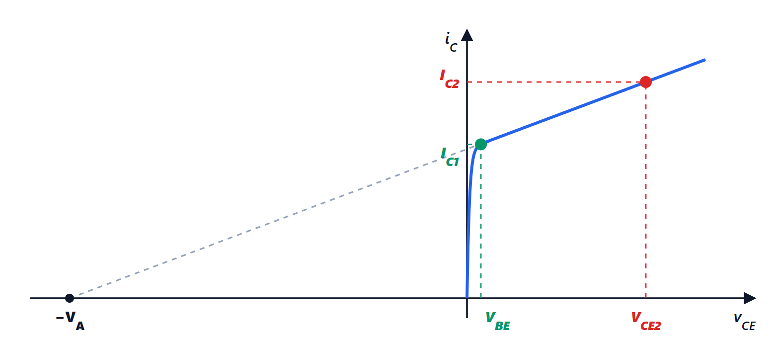
In the lesson the error due to base currents was computed assuming equal collector currents. With the Early effect they are not: for the same  , the collector current grows with
 :

The reference transistor, diode-connected, has  ; the output one has the
 imposed by the load. The bases are connected, so the exponential factor is the same and cancels in the ratio:
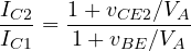
Bringing in the base currents: at the reference node  . With
 , where
 is the ratio just found,

For  the lesson’s formula is recovered. Example.
 V,
 V,
 V,
 :
 , and
 . The two errors have opposite signs and here the Early effect prevails: the output current is 2.2 % higher than the reference.
The mirror with a helper transistor
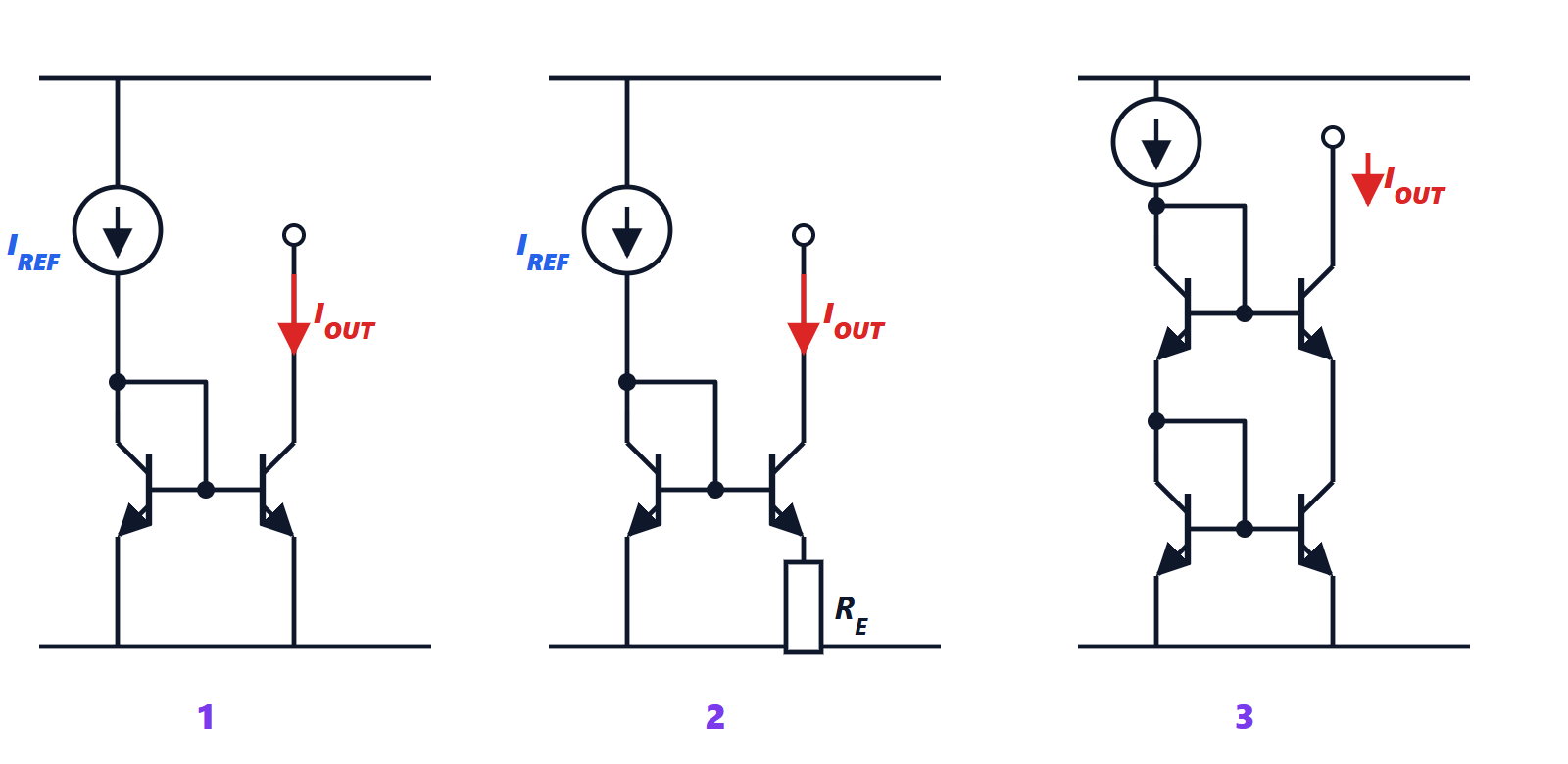
A third transistor Q3, an emitter follower, has its base on the collector of Q1 and its emitter on the bases of Q1 and Q2: it supplies the two base currents.
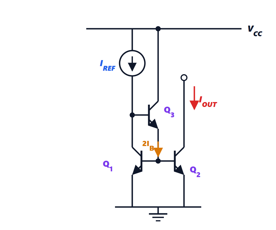
Theorem. With identical transistors,  , i.e. a relative error of about
 .
Proof. Q1 and Q2 have the same , so  and base currents
 each. These two currents,
 , come out of the emitter of Q3; its base current is
 , because the emitter current is
 times the base current. At the collector node of Q1, the reference splits between the collector of Q1 and the base of Q3:

hence the formula. ∎
With the error drops from 2 % to 0.02 %. The price is that the reference branch now has two in series, about 1.4 V, which reduce the headroom with low supplies.
The Wilson mirror
In the Wilson mirror the reference current enters the collector of Q1, which drives the base of Q3, the output transistor; the emitter of Q3 goes to the collector of Q2, diode-connected, whose base is joined to that of Q1. Q1 and Q2 thus form a simple mirror that “copies” the emitter current of Q3 into the reference branch.
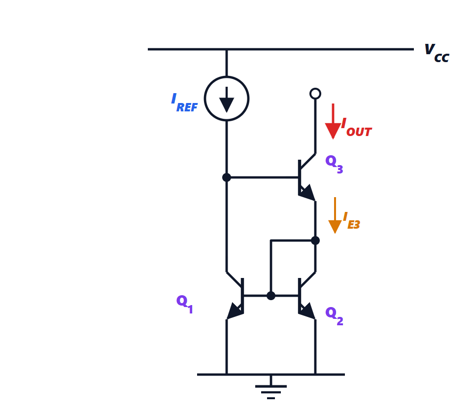
Theorem. With identical transistors,  , i.e. a relative error of about .
Proof. Let  be the collector current of Q1 and Q2, equal because they have the same (neglecting the Early effect). The collector node of Q2 receives the emitter current of Q3 and distributes it between the collector of Q2 and the two bases:
 . The output current is the collector current of Q3:
 . At the input node the reference splits between the collector of Q1 and the base of Q3:
 . Obtaining
 and substituting:

So  . ∎
The output resistance. If the voltage on the collector of Q3 rises, the output current tends to grow because of the Early effect. But that current, through Q2 and the Q2-Q1 mirror, increases the collector current of Q1, which takes current away from the base of Q3 and pulls it back: it is negative current feedback. Small-signal analysis (model with  ,
 ,
 , lesson on transistor amplifiers) gives
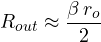
The factor 2 arises because half of the change in Q3’s collector current is returned as base current through the mirror, while the other half flows in Q3’s resistance : the feedback multiplies the resistance by about  rather than .
The output resistance of the cascode
The MOS cascode consists of two transistors in series: M1 at the bottom, with its gate at a fixed voltage, behaves as a current source with resistance  ; M2 above, with its gate at a fixed voltage, carries the current to the output.
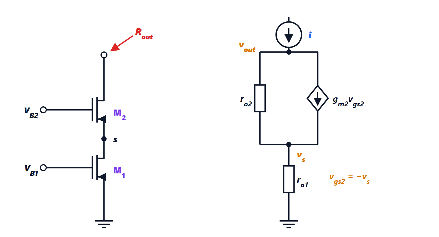
Theorem. The output resistance of the MOS cascode is

Proof. Apply to the output (the drain of M2) a small test current  , with all constant sources turned off: the gates are at fixed voltage, i.e. grounded for small signals. In M1 gate and source are grounded, so its
 source carries nothing, and M1 reduces to the resistance : the voltage at the source of M2 is
 . In M2 the gate is grounded, so
 , and its source carries the current
 from drain to source. By Kirchhoff’s current law at the drain node, the current in
 is
 , and the output voltage is

Dividing by gives the formula. ∎
The physical meaning: M2 holds its own source almost still, because any attempt to raise it reduces its  and hence the current. The resistance of M1 is “multiplied” by the intrinsic gain
 of M2, typically 20-100. The same calculation for the bipolar cascode gives
 : here the multiplication is limited by the base current of Q2, which escapes towards the fixed base.
The minimum voltage of the cascode
For all transistors to stay in saturation (in MOS,  ) the cascode needs a minimum voltage across it. In the “simple” cascode mirror the gates of the two diode-connected reference transistors, one above the other, fix the gate of M2 at
 . The source of M2 is therefore at
 , and the output drain must be at least
 above it:
 . M1 works with
 , more than necessary: one
 is wasted. The wide-swing cascode mirror biases the gate of M2 at
 with a dedicated branch, so that M1 works at the edge of saturation with
 , and the minimum voltage drops to
 . Example. With
 V and
 V: 0.9 V against 0.4 V, a decisive difference with a 1.2 V supply.
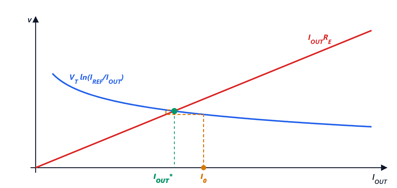
The Widlar mirror equation
For design, i.e. finding  given the current, the lesson’s formula applies directly. For analysis, i.e. finding
 given , the equation
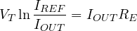
is transcendental: the unknown appears both inside the logarithm and outside, and cannot be isolated with algebra. It is solved by iteration. Rewritten as  , one starts from a trial value, puts it on the right and computes a new value, until it settles. Convergence is guaranteed because the right-hand side varies slowly: its derivative with respect to is
 , which at the solution equals
 , less than 1 in magnitude when the current ratio exceeds
 , i.e. always in the Widlar’s use cases (for a function with derivative less than 1 in magnitude the iteration is a contraction and converges, Numerical Calculus lesson on roots of functions). A complete example is in the exercises.
MOS mirrors and channel-length modulation
For the MOS mirror with channel-length modulation  , the same reasoning as for the Early effect gives

with  for the diode-connected transistor. Since is inversely proportional to the channel length, precision mirrors use long transistors (L several times the process minimum), or make
 equal to
 with a cascode or with an amplifier regulating the output voltage.
Exercises on the topic, with exam-style design and analysis problems, are on the exercise page linked at the top.