The bipolar junction transistor (BJT): operation, regions and biasing
Structure and operation in the active region, current gain, operating regions, the Early effect, stable biasing, the transistor as a switch and thermal runaway.
The bipolar junction transistor (BJT), invented in 1947-48 at Bell Labs, was the first semiconductor device able to amplify. In digital circuits it has since been replaced by the MOSFET, but it remains essential in analogue amplifiers, voltage references, radio-frequency and power circuits. In this lesson we see how it works, its equations and its operating regions.
The structure
An npn BJT has three regions: a heavily doped n emitter, a thin, lightly doped p base, and an n collector. So there are two junctions: base-emitter and base-collector. The pnp has the same regions with the types swapped, and voltages and currents of opposite sign.
The three regions are not symmetrical, and the differences are exactly what makes it work:
- the base is much thinner than the electron diffusion length;
- the emitter is much more heavily doped than the base.
Operation in the active region
In the active region the base-emitter junction is forward biased and the base-collector junction reverse biased.
- The forward-biased BE junction injects electrons from the emitter into the base, in an amount exponential in
 , as in a diode.
- In the base, electrons are minority carriers and diffuse. The base is so thin that almost none recombine.
- When they reach the edge of the BC junction, they meet the field of the depletion region, which sweeps them into the collector.
The result: the collector current is controlled by the base-emitter voltage and hardly depends on the collector voltage,

The BE junction also injects holes from the base into the emitter, and a few electrons recombine in the base: these two contributions make up the small base current, proportional to  :

 , the current gain, is typically 50 to 300. One also uses
 : with
 ,
 .
Why β is large. Applying diode theory to the BE junction, the ratio of the electron current injected into the base to the hole current injected into the emitter is about
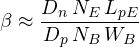
where  is the base width. A heavily doped emitter (
 ) and a thin base (small ) give a large : this is why the structure is not symmetrical.
Operating regions
| Region | BE junction | BC junction | Behaviour |
|---|---|---|---|
| cut-off | reverse | reverse | no current, open switch |
| active | forward | reverse |  , amplifier |
| saturation | forward | forward |  V, closed switch |
| reverse active | reverse | forward | like active, but with small |
Output characteristics and the Early effect
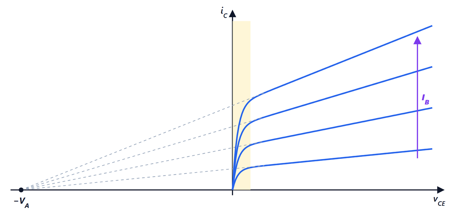
In the active region the curves are not perfectly flat: as  increases, the BC depletion region extends into the base, the effective base gets thinner and the current rises slightly. This is the Early effect, described by
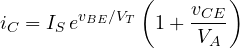
with  , the Early voltage, between 50 and 200 V. The transistor therefore has a finite output resistance
 , which limits amplifier gain.
Biasing
To use the transistor as an amplifier you must set an operating point in the active region. The problem is that varies a lot from one device to another and with temperature.
- With a single base resistor from
 :
 and
 . If doubles,
 doubles too: to be avoided.
- With a divider and an emitter resistor: a divider sets the base voltage
 , and the current is
 , independent of β. With
 V and
 kΩ,
 mA whatever the transistor. The emitter resistor also provides feedback: if the current tends to rise,
 rises, falls and the current drops.
Example. With the circuit just described,  V and
 kΩ:
 mA, 4.7 V drops across the collector resistor and 2.3 V across the emitter resistor, so
 V. The transistor is in the active region, with room for the signal to swing both ways.
The transistor as a switch
Between cut-off and saturation the BJT acts as a controlled switch. To drive a 100 mA relay with a transistor whose minimum is 50 you need  mA; to be sure of saturation one designs with a “forced” of 10 to 20, that is 5 to 10 mA of base current. In saturation the base stores charge, and turn-off is slower than turn-on: one of the limits of BJTs in fast circuits.
Temperature
As in the diode, at constant current decreases by about 2 mV/°C; at constant voltage the current increases. In a power transistor, heating raises the current, which raises the temperature further: this is thermal runaway, prevented precisely by the emitter resistor and an adequate heat sink. Conversely, in integrated circuits the temperature dependence of , combined with that of  , is used to build stable “bandgap” voltage references, at about 1.2 V.