CMOS logic: inverter, logic gates, power and scaling
The CMOS inverter and its characteristic, NAND and NOR gates, dynamic power with proof, speed, Moore's law, FinFETs and integrated circuit fabrication.
Almost all digital electronics, from microcontrollers to the processors in phones and servers, is built with a single technology: CMOS (complementary MOS), which uses pairs of nMOS and pMOS transistors. Its decisive advantage is that at rest it consumes almost nothing. In this lesson we look at the CMOS inverter, how logic gates are built, where power consumption comes from and how integrated circuits have grown.
The CMOS inverter
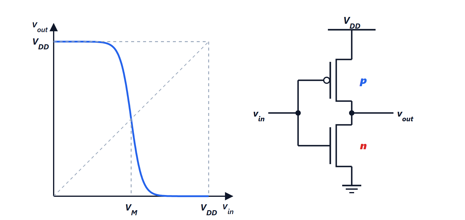
A pMOS connected between the supply  and the output, an nMOS between the output and ground, the two gates tied together to the input.
- Low input (0 V): the nMOS is off (
 ), the pMOS is on (its gate is volts below its source). The output is connected to : high.
- High input (): the nMOS is on, the pMOS off. The output is connected to ground: low.
In both stable states one of the two transistors is off, so no current flows between supply and ground: static power is zero, apart from small leakage currents. And the outputs reach exactly 0 and , which makes the logic levels very robust.
The transfer characteristic
In the transition region both transistors conduct and are in saturation: there the circuit is an inverting amplifier with very high gain, and the output goes from high to low over a narrow range of input voltage. The logic threshold  is the point where
 , with equal currents in the two transistors. To place it at
 , the pMOS is made wider than the nMOS, by roughly the mobility ratio, to compensate for the slowness of holes.
The high gain makes the logic regenerative: a slightly degraded signal at the input comes out clean, and disturbances do not build up along a chain of gates. The noise margins say how much a level can be disturbed without being misread.
Logic gates
Every CMOS gate has a pull-down network of nMOS transistors to ground and a pull-up network of pMOS transistors to the supply, complementary to each other:
- NAND: nMOS in series (the output goes to ground only if all inputs are high), pMOS in parallel;
- NOR: nMOS in parallel, pMOS in series.
Natural CMOS gates are inverting; AND and OR are obtained by adding an inverter. With NAND gates alone, or NOR gates alone, any logic function can be built: that is why they are called universal gates. A flip-flop is made of gates with feedback, and an SRAM memory cell of six transistors: two inverters in a loop and two access transistors.
Dynamic power
Power is consumed at every switching event. A gate’s output drives a capacitance  : the gates of the following stages and the wiring.
Theorem. A gate switching at frequency  dissipates an average power

where  is the fraction of cycles in which the output goes from low to high (the activity factor).
Proof. When the output rises, the pMOS charges from 0 to : the supply delivers the charge  , that is the energy
 . Half of it,
 , stays in the capacitor; the other half is dissipated in the pMOS resistance, whatever its value. When the output falls, the nMOS discharges the capacitor and dissipates the stored energy. So a full cycle loses
 , and with
 cycles per second we get the formula. ∎
Example. A processor with 100 nF of total switched capacitance,  V, 3 GHz and
 :
 W. The dependence on the square of the voltage explains why supplies have dropped from 5 V to below 1 V, and why processors lower voltage and frequency when the workload is light.
On top of this there is the brief short-circuit current during the transition, when both transistors conduct together, and subthreshold leakage, which in modern processes is a significant part of total consumption.
Speed
A gate’s delay is the time needed to charge or discharge the output capacitance with the transistor current:  . Smaller transistors have smaller capacitances and hence faster gates; lower voltages reduce power but also current, and therefore speed. Designing a digital circuit is a constant trade-off between these two aspects.
Miniaturisation
For decades transistor dimensions shrank by about 0.7 times roughly every two years, doubling the number of transistors per area: this is Moore’s law, an observation from 1965 that became the industry’s roadmap. As long as dimensions and voltages shrank together (Dennard scaling), each generation was denser, faster and used less energy per operation.
Around 2005 the voltage stopped falling, because the threshold could not be lowered without increasing subthreshold leakage too much. Processor frequency levelled off at a few gigahertz, and the extra transistors were used for more cores. To control the channel better, the gate moved from the planar structure to the three-dimensional FinFET (the channel is a fin wrapped by the gate on three sides) and then to gate-all-around, with the channel completely surrounded.
How an integrated circuit is made
On a wafer of single-crystal silicon a sequence of steps is repeated many times:
- oxidation or deposition of a layer (insulator, polysilicon, metal);
- photolithography: a photosensitive resist is exposed through a mask, and after development it protects only some areas; the most advanced processes use extreme ultraviolet light at 13.5 nm;
- etching of the unprotected areas;
- ion implantation of dopants and annealing to activate them.
Transistors are built in the lowest layers; above them there are up to about fifteen levels of copper interconnect, separated by insulators. Finally the wafer is tested, diced into individual chips and packaged.