Design flow, timing analysis and low-power design
From RTL to GDS, functional verification and synthesis, static timing analysis and corners, DRC, LVS and extraction, clock gating, multiple thresholds and power gating with the break-even time proved.
A modern processor is not drawn transistor by transistor: billions of devices are obtained from a high-level description through a chain of electronic design automation (EDA) programs. Every step transforms the design and every step must be verified, because an error discovered after manufacturing costs millions and months. In this lesson we look at the digital design flow from the RTL description to the file for the fab, static timing analysis, physical verification, and low-power design techniques with the proof of the power-gating break-even time.
The flow
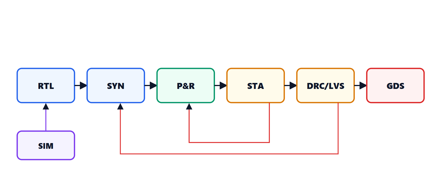
- Specification and architecture: what the chip must do, with what performance, power and cost.
- RTL: the logic is described at the register-transfer level in a language such as Verilog or VHDL (Digital Systems Electronics lesson on FPGAs and Verilog).
- Functional verification: simulations with millions of test cases generated randomly and in a directed way, assertions, and formal verification that mathematically proves some properties. In large projects verification employs more engineers than design itself.
- Logic synthesis: a program translates the RTL into a network of gates taken from a standard cell library of the process, optimising for area, speed and power.
- Placement and routing: cells are placed on the chip and connected with the metal levels; the clock tree is built, which carries the clock to millions of registers with almost equal delays.
- Timing closure and physical verification, seen below.
- Tape-out: the final layout, in GDS format, goes to the fab for mask production.
Static timing analysis
Instead of simulating all possible signals, impossible for billions of gates, static timing analysis (STA) computes for each path between two registers the maximum and minimum delay, adding up the delays of the cells and of the interconnects extracted from the physical layout (lessons on delays and interconnects). For each path it checks the setup condition (the data arrives in time before the clock edge) and the hold condition (it does not change too soon after), already seen in the Digital Systems Electronics lesson on timing. The slack of a path is the time to spare; negative slack is a violation to be fixed by resizing cells, adding repeaters or changing the logic.
The analysis is repeated at all process, voltage and temperature corners: slow transistors at low voltage and high temperature for setup, fast ones for hold. With the variability of modern processes statistical analyses are also used.
Physical verification
- DRC (design rule check): does the layout respect the thousands of geometric rules of the process, minimum spacings and widths, metal densities?
- LVS (layout versus schematic): does the circuit extracted from the layout coincide with the intended one, transistor by transistor and connection by connection?
- Parasitic extraction: resistances and capacitances of all interconnects, for timing analysis and analogue simulations.
- Power analysis: voltage drops, electromigration (lesson on interconnects).
Low-power design
Dynamic power is  and static power comes from leakage currents (Computer Architecture lesson on energy and lesson on the nanometre MOSFET). The main techniques:
- clock gating: the clock tree alone consumes 30-40 % of dynamic power, because it switches every cycle. The clock of registers that need not change is stopped, reducing the activity factor;
- multiple thresholds: high-threshold cells, slower but with ten times less leakage, on paths with slack; low-threshold cells only on critical ones;
- voltage islands and DVFS: blocks supplied at different voltages, adjusted to the load;
- power gating: a switch removes the supply from an idle block, eliminating leakage too.
Switching off has a cost, though: the state must be saved, and at power-up all the block’s capacitances must be charged.
Theorem. If switching a block off and on costs energy  and the block, on but idle, dissipates leakage power
 , power gating saves energy only if the idle period exceeds the break-even time

Proof. Leaving the block on for a time  costs
 ; switching it off costs (neglecting the small residual leakage of the switch). Switching off pays if
 , i.e.
 . ∎
The chip’s power controller estimates how long the idle period will last and decides accordingly; in phones blocks are switched off and on thousands of times a second.
Analogue and mixed-signal design
Analogue blocks (lessons on the integrated op-amp and on noise) are still largely designed by hand, with transistor-level simulations at all corners and Monte Carlo statistical analyses of mismatch, and are laid out carefully. Integration with the digital part requires isolating sensitive circuits from the noise digital circuits inject into the substrate and supplies (Electromagnetic Compatibility lessons). Automatic generation programs and machine learning techniques are entering this field too, but the designer’s experience still counts a great deal.