The nanometre MOSFET: velocity saturation, subthreshold and variability
Velocity saturation, short-channel effects and DIBL, the 60 mV per decade subthreshold slope proved, the end of voltage scaling, variability.
The square-law MOSFET model (Electronic Devices lesson on the MOSFET) describes transistors a few micrometres long well. In today’s transistors, with channels a few tens of nanometres long, new effects appear that change the rules of digital and analogue design. In this lesson we look at velocity saturation, short-channel effects, subthreshold conduction with the proof of the 60 mV per decade limit, its consequences on the supply voltage, and variability.
Velocity saturation
In the classic model electrons in the channel move with a velocity proportional to the electric field,  . But the field in a 20 nm channel with 0.8 V is tens of kilovolts per centimetre, and beyond about
 V/cm the velocity stops growing: it saturates at about
 cm/s, because the electrons give their energy to the lattice. The current no longer grows with the square of the gate drive, but roughly linearly:

with  the gate capacitance per unit area. The consequence is that shortening the channel further no longer increases the current as before, and the gain of analogue circuits, linked to transconductance, suffers too.
Short-channel effects
When the channel is short, the drain voltage influences the potential barrier near the source, which should be controlled by the gate alone. This gives rise to:
- drain-induced barrier lowering (DIBL): the threshold voltage drops as
 increases, and the off-state current grows;
- channel-length modulation: in saturation the current keeps growing with , and the transistor’s output resistance is low. The intrinsic gain
 , which was a few hundred in micrometre transistors, drops to 10-20.
The remedy is to give the gate stronger control over the channel: high-dielectric-constant insulators, and above all FinFET and gate-all-around structures (lesson on the process).
Subthreshold conduction
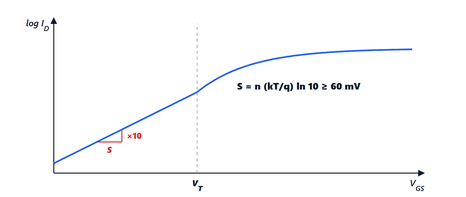
Below the threshold voltage the transistor is not completely off: electrons that overcome the barrier by thermal agitation produce a current that grows exponentially with the gate voltage, as in a diode.
Theorem. The subthreshold slope, i.e. the increase of  needed to multiply the current by ten, is

with  , and therefore it cannot go below 60 mV per decade at room temperature.
Proof. The subthreshold current is dominated by electrons with enough energy to overcome the barrier between source and channel. By Boltzmann statistics their density is proportional to  , where
 is the surface potential of the channel. The gate controls through a capacitive divider between the oxide capacitance and that of the depletion region, so varies as
 , with
 . The current is then
 . Multiplying it by 10 requires
 to increase by
 , i.e.
 . With
 mV at 300 K,
 mV. ∎
The end of voltage scaling
The result has an enormous consequence. An off transistor must conduct much less than an on one: typically 5-6 decades of on-to-off current ratio are needed. With 60-80 mV per decade, the threshold voltage cannot go below 0.3-0.4 V, and the supply below 0.7-0.8 V. Every 60-80 mV less of threshold multiplies the leakage current by ten, which in a chip with billions of transistors becomes static power (Computer Architecture lesson on energy). That is why the supply voltage, which fell from 5 V to about 1 V between 1990 and 2005, has been almost stuck since then, and Dennard scaling has ended.
Beating 60 mV per decade would require a mechanism other than the thermal barrier: tunnel field-effect transistors and negative-capacitance transistors are the subject of research, but not yet of production.
Variability
In a 20 nm by 20 nm transistor there are a few tens of dopant atoms in the channel, and their number and position change from one transistor to another: the threshold voltage varies randomly even between identical neighbouring transistors. To this are added the irregularities of the edges drawn by lithography and the thickness of the layers. Variability forces design with margins: SRAM memories, which use the smallest possible transistors, must work even with the worst transistor among billions, and in analogue circuits the matching between transistors becomes a design parameter (lesson on noise and matching).