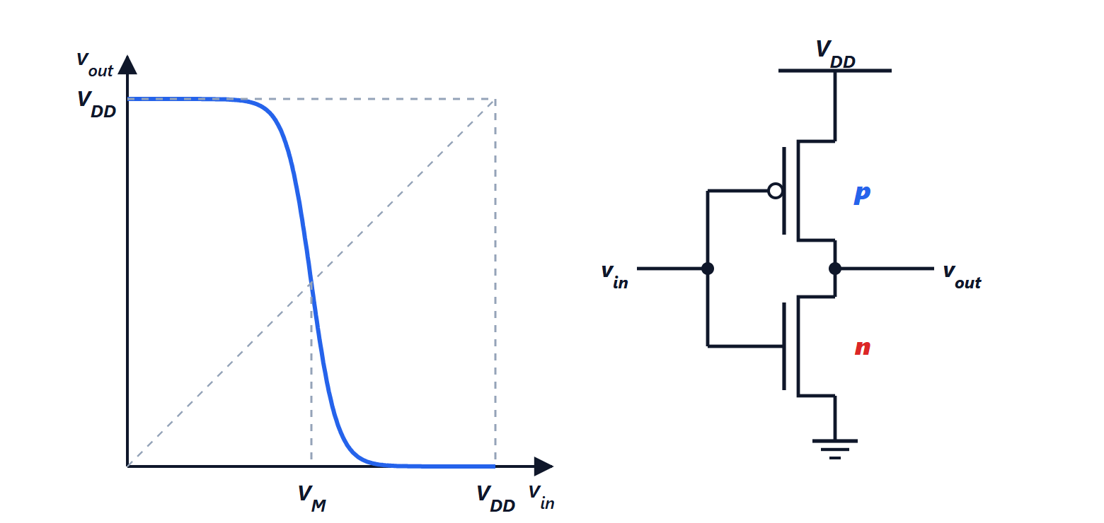
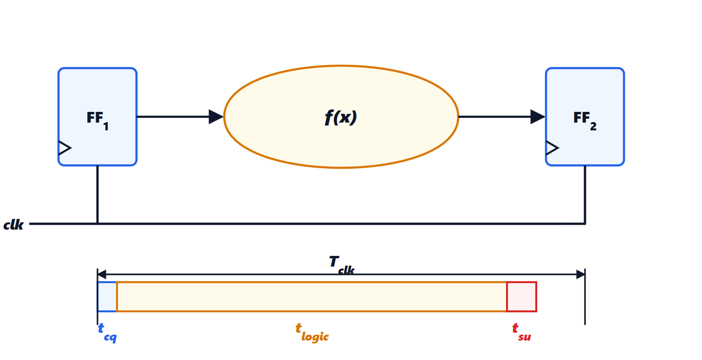
Integrated circuit fabrication: lithography, FinFETs and yield
Process steps, lithography and the Rayleigh criterion, EUV, FinFET and gate-all-around, Poisson yield proved, cost per die with an example, chiplets.
A modern processor contains tens of billions of transistors on a few square centimetres of silicon, with features a few nanometres across, and is produced in millions of units. The Electronic Devices lesson on CMOS logic introduced fabrication. Here we look at it more closely: the process steps, lithography and its resolution limit, the structures of modern transistors, and yield, with the proof of the Poisson model and its effect on the cost of a chip, which explains why large chips are now split into chiplets.
The process steps
One starts from a wafer, a disc of ultra-pure single-crystal silicon 300 mm in diameter. Circuits are built on it layer by layer, repeating a few basic operations hundreds of times:
- oxidation and deposition of insulating, conducting and semiconducting layers;
- lithography: a light-sensitive resist is spread, exposed through a mask carrying the layer’s pattern, and developed;
- etching, chemical or by plasma, removing the material not protected by the resist;
- doping by ion implantation, followed by rapid annealing that repairs the lattice and activates the dopant atoms;
- metallisation: copper interconnects, up to 15-20 stacked levels separated by low-dielectric-constant insulators, made with the damascene process (trenches are dug in the insulator, filled with copper and everything is planarised by chemical-mechanical polishing).
The lower part, with the transistors, is called the front end; the upper part, with the interconnects, the back end. At the end the circuits are tested on the wafer, which is diced into individual dies, then packaged.
Lithography
The minimum size that can be printed is limited by the diffraction of light. The Rayleigh criterion gives the resolution
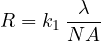
with  the wavelength,
 the numerical aperture of the optics and
 a process factor, which the most refined techniques push towards the theoretical limit of 0.25. For years 193 nm ultraviolet light was used, improved with immersion in water (which raises above 1) and with multiple patterning (splitting a dense pattern over two or four masks). Today the finest layers are printed with extreme ultraviolet (EUV) at 13.5 nm, produced by tin droplets hit by a laser and focused with mirrors, because at that wavelength no material is transparent. EUV machines are among the most complex instruments ever built.
Process names (“3 nm”, “2 nm”) no longer correspond to a physical dimension: they are commercial labels for a generation. The minimum distance between transistor gates is a few tens of nanometres.
Modern transistors
The planar MOSFET can no longer control the channel when it is too short (lesson on the nanometre MOSFET). Since 2011 the FinFET has been used: the channel is a thin vertical silicon “fin”, wrapped by the gate on three sides, which controls it much better. The most recent generations move to gate-all-around (nanosheet) transistors, with the channel made of thin stacked horizontal layers completely surrounded by the gate. The gate insulator is no longer silicon dioxide but a high-dielectric-constant material, with a metal gate, to obtain strong coupling without tunnelling leakage currents.
Yield
Not all the dies on a wafer work: dust particles, crystal defects, lithography errors ruin some circuits. The fraction of good dies is the yield, and it is decisive for cost.
Theorem. If fatal defects are distributed randomly and independently over the wafer, with mean density  per unit area, the yield of a die of area
 is

Proof. With independent, uniform defects, the number of defects falling in an area follows a Poisson distribution with mean  : the probability of finding exactly
 is
 . The die works if it contains none:
 . ∎
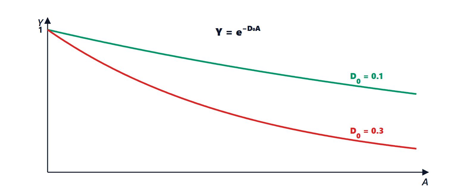
In reality defects tend to cluster and the Poisson model is somewhat pessimistic for large dies; variants are used (Murphy, negative binomial), but the exponential trend remains.
Example. A 300 mm wafer holds about 640 dies of 1 cm² and about 143 dies of 4 cm² (the edges waste more space with large dies). With  per cm² the yields are 90.5 % and 67 %: the good dies are about 580 and about 96. The 4 cm² chip has four times the area but costs about six times as much. That is why the largest processors are now built from several chiplets: small high-yield dies, tested separately and assembled together on a substrate or a silicon interposer with very dense connections. Different processes can also be mixed, the most advanced for logic and a cheaper one for the interfaces.