Timing of synchronous circuits and clock domains
The setup constraint and maximum frequency with an example, the hold constraint, clock skew and jitter, pipelining, static timing analysis, clock domain crossing and asynchronous FIFOs.
In a synchronous circuit all flip-flops change state together, on the edge of a single clock, and between one edge and the next the combinational networks have time to compute the new values. This discipline makes huge designs manageable, but it imposes precise timing constraints. In this lesson we derive a circuit’s maximum frequency, the hold constraint, the effect of clock skew, pipelining and passing data between different clock domains.
The path between two flip-flops
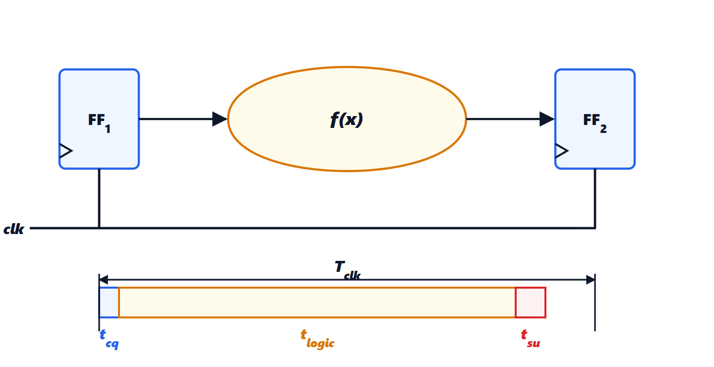
On edge  the first flip-flop changes its output after
 ; the new value goes through the logic in at most
 ; it must reach the second flip-flop at least
 before edge
 .
Theorem (setup constraint). The circuit works if

The proof is the reasoning just made: data launched on one edge must be stable at the next flip-flop’s input before the following edge.
Example.  ns,
 ns,
 ns:
 ns,
 MHz. The path with the largest sum is the critical path, and it sets the frequency of the whole circuit: it does not matter how fast all the others are.
The hold constraint
There is also the opposite risk: that the new data arrives too early and overwrites the value the next flip-flop is still capturing on the same edge. The data at the second flip-flop must stay stable for  after the edge:

The hold constraint does not depend on frequency: if it is violated, the circuit does not work even with a very slow clock. It typically happens with two flip-flops connected directly, with no logic in between, and with the clock reaching the second one late. Design tools fix it by inserting delay buffers on paths that are too short.
Clock skew
The clock does not arrive at all flip-flops at the same instant: the distribution network has different delays to different points of the chip. The difference is the skew  . If the clock reaches the receiving flip-flop later, the setup constraint improves and the hold constraint worsens; if earlier, the opposite:

Then there is jitter, the random variation of the period from cycle to cycle, which always eats into the margin. In processors the clock network is designed as a balanced tree or a grid, and it consumes a significant share of the chip’s power.
Pipelining
If the critical path is too slow for the desired frequency, it is broken by inserting registers in the middle: this is pipelining, the same seen for processors in Computer Architecture. A 4 ns logic split into two 2 ns stages runs at twice the frequency: each data item takes two cycles (the latency grows) but a new one enters every cycle (the throughput doubles). It is the main technique for high frequencies in FPGAs and signal-processing circuits.
The reverse is possible when an operation is too long but rare: a multicycle path is declared, allowed two or more periods, and the verification tools take it into account.
Timing verification
A chip has millions of paths. They are not verified by simulation, but with static timing analysis: a program computes the maximum and minimum delays of every path, including process, voltage and temperature variations (the “corners”), and reports any negative margins (slack). The designer declares the constraints: the frequency of each clock, input and output delays, exceptions.
Clock domains
Different systems have different clocks: a USB interface, the memory, the processor. A signal passing from one domain to another is, for the receiving domain, asynchronous, and must be handled as seen in the lesson on flip-flops:
- a single bit goes through a two-flip-flop synchroniser;
- a multi-bit word cannot be synchronised bit by bit, because the bits might be captured in different cycles and form a value that never existed. So an asynchronous FIFO is used, with its pointers in Gray code (only one bit changes at each increment, so a value captured mid-transition is still either the old or the new one), or a handshake protocol that holds the data still until the other side confirms it has read it.
Clock domain crossing errors are among the most insidious in digital electronics: they do not show up in simulation, appear rarely and only on some devices, which is why dedicated verification tools exist.