Semiconductor memories: SRAM, DRAM and flash
Array organisation with decoder and sense amplifiers, the six-transistor SRAM cell, the DRAM cell and refresh, NOR and NAND floating-gate flash, comparison and new technologies.
Semiconductor memories are the most-produced integrated circuits: the RAM of computers, the flash of phones and USB sticks, the caches inside processors. They are regular arrays of millions or billions of identical cells, and the cell type decides speed, density, power and whether data survive with the power off. In this lesson we look at the organisation of a memory and at SRAM, DRAM and flash cells.
Organisation
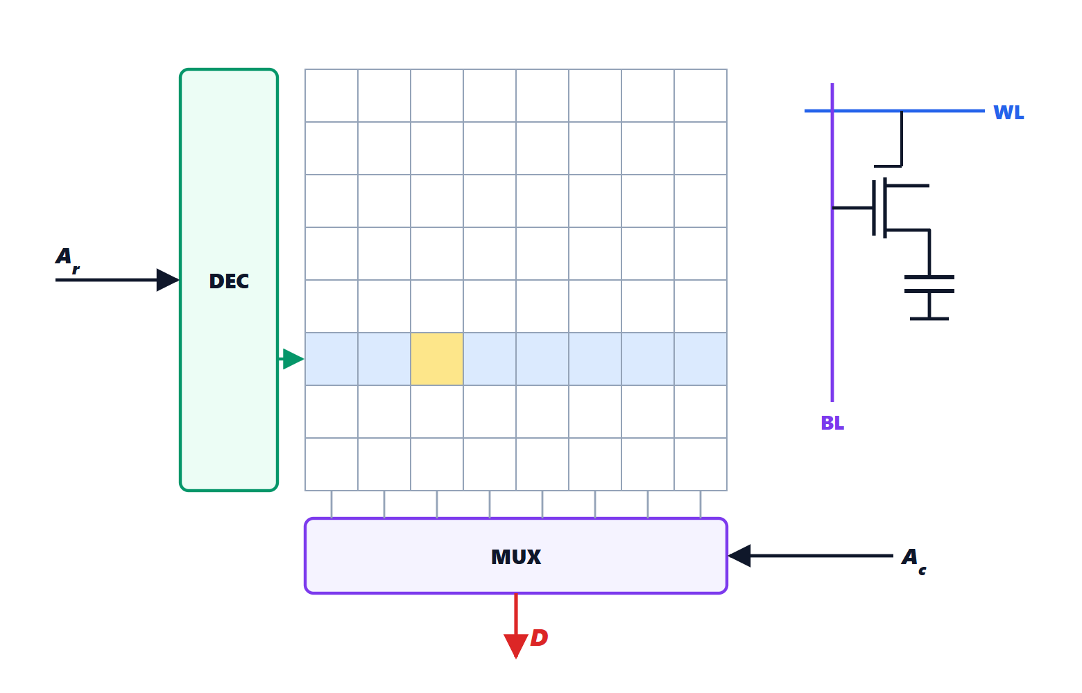
The cells are arranged in a square array, more compact than a long row. The address splits into two parts:
- the row address goes to a decoder (lesson on combinational networks) that activates a single word line: all the cells of that row connect to their bit lines;
- the column address drives a multiplexer that picks, among all the bit lines, those of the requested data.
The signals on the bit lines are tiny (the cell is minuscule and the line long and capacitive), so at the bottom of each column there is a sense amplifier, usually a latch that amplifies a difference of a few millivolts up to the logic level.
SRAM
The SRAM (static) cell is made of six transistors: two CMOS inverters in a loop, the latch seen in the lesson on flip-flops, and two access transistors connecting it to the two bit lines (true and complement) when the word line is active. As long as it is powered it holds the data with no further help, reads non-destructively and very quickly: it is the memory of caches and registers. Its drawback is area: six transistors per bit. That is why caches are a few megabytes even in the largest processors.
DRAM
The DRAM (dynamic) cell is as simple as can be: one transistor and one capacitor. The bit is the capacitor’s charge, a few tens of femtofarads. To read it, the word line is activated and the capacitor shares its charge with the bit line, moving its voltage by a few millivolts; the sense amplifier detects the shift.
Two consequences:
- reading is destructive: after reading, the amplifier must write the row back;
- the capacitor slowly discharges through transistor and junction leakage: every cell must be periodically read and rewritten (refresh), typically every 64 ms. With 8192 rows to refresh, one refresh command every 7.8 µs.
DRAM is dense and cheap, and it is the main memory of every computer and phone. Modern DRAMs (DDR4, DDR5, LPDDR) are organised in many independent banks and transfer data on both clock edges, at thousands of megatransfers per second, but the time to access a new row is still around 15 ns: that is why caches are needed.
Flash
Non-volatile memories keep data without power. In flash each cell is a MOSFET with a second gate, the floating gate, completely insulated in the oxide. Applying high voltages (10 to 20 V) pushes electrons into the floating gate by tunnelling, or removes them; the trapped charge shifts the transistor’s threshold voltage, and reading whether it conducts at an intermediate voltage gives the bit. The electrons stay trapped for years.
- NOR flash connects cells in parallel: fast random reads, used for microcontroller code, which is executed directly from it.
- NAND flash connects cells in series in strings: much denser and cheaper, read and written by pages (a few kilobytes) and erased by blocks (hundreds of kilobytes). It is the memory of SSDs, cards and phones.
To increase density each cell stores several bits by distinguishing several charge levels (MLC 2 bits, TLC 3, QLC 4) and cells are stacked vertically, more than two hundred layers (3D NAND). The price is endurance: every program and erase cycle damages the oxide a little, and a cell withstands from a few thousand to a hundred thousand cycles. The SSD controller spreads writes over all cells (wear levelling) and corrects errors with powerful codes.
Comparison
| Memory | Cell | Volatile | Speed | Density | Use |
|---|---|---|---|---|---|
| SRAM | 6 transistors | yes | highest | low | caches, registers |
| DRAM | 1 transistor + 1 capacitor | yes, with refresh | high | high | main memory |
| NOR flash | 1 floating-gate transistor | no | fast read, slow write | medium | microcontroller code |
| NAND flash | cells in series, several bits per cell | no | by pages | highest | SSDs, phones, cards |
| EEPROM | 2 transistors | no | slow | low | small configuration data |
New technologies try to combine speed and non-volatility: magnetic (MRAM), phase-change and resistive memories. MRAM is already used in some microcontrollers and in the caches of low-power systems.