FPGAs and hardware description languages
Look-up tables and logic blocks, programmable interconnect and dedicated blocks, when to use an FPGA, a counter in Verilog, the design flow from simulation to programming.
A custom integrated circuit (ASIC) is the most efficient way to implement a digital function, but designing and producing it costs millions and takes months, and once made it cannot be fixed. FPGAs (Field Programmable Gate Arrays) are chips full of programmable logic blocks and connections, configured in a few seconds to become any digital circuit. In this lesson we see how they are built, how a circuit is described with a hardware description language and the design flow.
The logic block
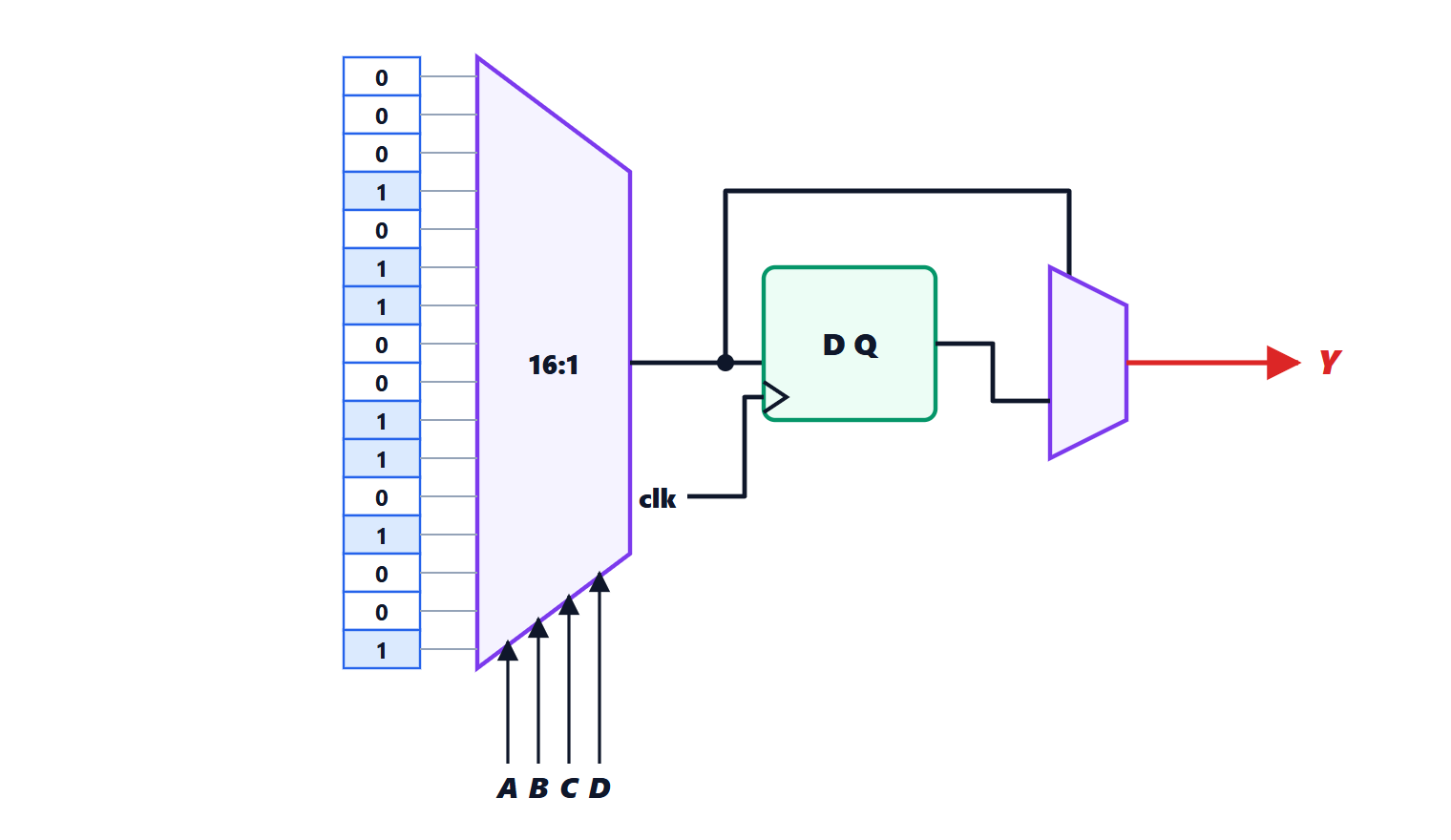
The heart of an FPGA is the look-up table (LUT): a small memory of  bits and a multiplexer with
 select inputs. As seen in the lesson on combinational networks, a multiplexer with the right constants on its data inputs implements any function of its select variables: a 4-input LUT can be any of the
 functions of 4 variables, by writing the truth table column into the memory. Modern FPGAs use 6-input LUTs.
Each LUT is followed by a flip-flop, which can be used or bypassed: with thousands or millions of these blocks, combinational and sequential networks of any size are built.
The rest of the FPGA
- Programmable interconnect: a network of lines and switches, controlled by memory cells, linking the blocks together. It takes most of the chip’s area and delay.
- Input and output blocks, configurable for different electrical standards (levels, impedances, serial transceivers at tens of gigabits per second).
- Dedicated blocks, far more efficient than LUTs for their tasks: block memories, multiply-accumulate units (DSP) for signal processing, clock generators (PLLs), and in some models entire ARM processors.
The configuration sits in SRAM cells and is lost at power-off: at power-up the FPGA loads it from an external flash memory. There are also FPGAs with internal flash configuration, which start instantly.
When to use them. FPGAs are used for ASIC prototypes, for low-volume products (instruments, telecom equipment, aerospace systems), when standards change and the circuit must be updated in the field, and when massively parallel processing with deterministic latency is needed: dozens of simultaneous filtering channels, video processing, high-speed motor control, computation acceleration in data centres. Compared with an ASIC they use more power, cost more per unit and are slower; compared with a processor they do in parallel and in one cycle what software would do in sequence.
Hardware description languages
A circuit with millions of gates is not drawn: it is described in a language such as VHDL or Verilog (and its successor SystemVerilog). They look like programming languages, but they describe hardware, in which everything happens in parallel. An 8-bit counter with reset and enable, in Verilog:
module counter (
    input  wire       clk,
    input  wire       rst,       // synchronous reset
    input  wire       en,        // enable
    output reg  [7:0] q
);
    always @(posedge clk) begin
        if (rst)
            q <= 8'd0;
        else if (en)
            q <= q + 8'd1;
    end
endmodule
The always @(posedge clk) block describes flip-flops changing on the rising edge; the <= (non-blocking) assignment means that all registers update together, as in real hardware. The synthesis tool recognises in these lines a register of 8 flip-flops, an adder and two multiplexers.
The design flow
- Description of the behaviour in HDL.
- Simulation: a testbench, also written in HDL, applies inputs and checks outputs. This is where most bugs are found, and where most time is spent.
- Synthesis: the tool translates the description into a network of LUTs, flip-flops and dedicated blocks.
- Place and route: each element is assigned to a physical block of the chip and the connections are routed.
- Static timing analysis (lesson on timing): checking that every path meets the required frequency.
- Programming the chip with the configuration file (bitstream) and testing on hardware, with integrated logic analysers recording internal signals.
The same flow, with cell libraries in place of LUTs and extra steps for fabrication, is used to design ASICs and processors. The decisive difference is that on an FPGA a bug is fixed in minutes, while on a chip already produced it can cost months and millions: that is why ASIC designs are almost always tried out first on large FPGAs.