BJT logic gates: RTL, DTL, TTL 7400, Schottky and ECL
The transistor as a switch and saturation, RTL NOR and fan-out proved, DTL, the TTL 7400 NAND state by state with its totem pole, levels, noise margins and current spike simulated with SPICE, Schottky TTL, ECL which never saturates, comparison with CMOS.
Before CMOS, digital logic was made of bipolar transistors. The RTL, DTL, TTL and ECL families built computers from the 1960s to the 1980s (the guidance computer of the Apollo missions was made entirely of RTL NOR gates), and TTL set the 5 V logic levels and the conventions still in use today. This lesson shows how they work, with hand calculations and SPICE simulations: the transistor as a switch and the problem of saturation, the RTL NOR gate and its fan-out, DTL, the TTL 7400 NAND with its totem-pole output stage, the Schottky variants, ECL which never saturates, and the comparison with CMOS.
The idea in simple words
In a logic gate the transistor does not amplify: it acts as a switch. Off, it leaves the output high; on, it pulls it towards ground. The bipolar logic families are different ways of driving these switches and of connecting gates together. The problems are always the same three: how many gates an output can drive (the fan-out), how much disturbance an input can tolerate without error (the noise margin), and how quickly the switch opens and closes (the propagation delay), paying in return a certain power consumption. Each new family improved one of these aspects; ECL, to be extremely fast, gave up switching its transistors fully off.
The transistor as a switch
The BJT has two states useful for logic: cut-off ( V or so, no current, output high) and saturation (base and collector both forward biased,
 between 0.1 and 0.2 V, output low). To saturate the transistor the base current must exceed the one that would be needed in the active region:
 . The ratio between the two is called overdrive.
Saturation has a cost: the base fills up with excess charge, and to switch the transistor off this charge must first be removed. The resulting storage time is often the longest term in the delay of a saturating gate: this is why fast families avoid saturation (Schottky, ECL).
RTL
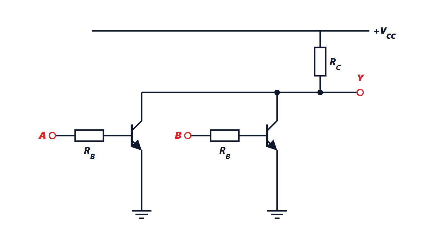
Resistor-Transistor Logic is the simplest: each input drives a transistor through a base resistor, and the collectors are in parallel on a common resistor (figure). If at least one input is high, its transistor saturates and the output goes low; the output is high only if all inputs are low: it is a NOR. Typical values of the family:  V,
 Ω,
 Ω.
The weak point is the high level. When the output is high, the resistor  must supply base current to all the connected gates, and each load is a resistor
 in series with a base-emitter junction (about 0.75 V).
Theorem. With  equal loads the high output voltage of the RTL gate is

Proof. The base resistors of the loads are in parallel ( ) and all end at the junction voltage
 . With the gate transistor off, and form a divider between
 and . ∎
| loads N | computed V_OH | V_OH with SPICE | margin above 0.75 V |
|---|---|---|---|
| 1 | 1.93 V | 1.94 V | 1.18 V |
| 2 | 1.49 V | 1.51 V | 0.74 V |
| 5 | 1.10 V | 1.11 V | 0.35 V |
| 10 | 0.94 V | 0.95 V | 0.19 V |
With ten loads the high level is less than 0.2 V above the threshold: a small disturbance is enough to cause an error. The practical fan-out of RTL is 4 or 5 gates, and the noise margins are small in any case.
DTL
Diode-Transistor Logic moves the logic function into diodes. Each input is the cathode of a diode; the anodes are joined and fed by a resistor; from that node, through two diodes in series, the base of the output transistor is driven. If an input is low, its diode conducts and holds the node at about 0.9 V: the two series diodes and the base are not enough to conduct (it would take  V), the transistor is off and the output high. Only if all inputs are high does the current go into the base, the transistor saturates and the output goes low: it is a NAND.
Two advantages over RTL: the series diodes raise the input threshold to about 1.4 V, improving the noise margin; and a high output has to supply almost no current to the loads (their input diodes are reverse biased), so the high level does not collapse with fan-out. A low output, instead, must sink the current flowing out of every low input: the fan-out is limited by the current the saturated transistor can sink.
TTL: the 7400 NAND
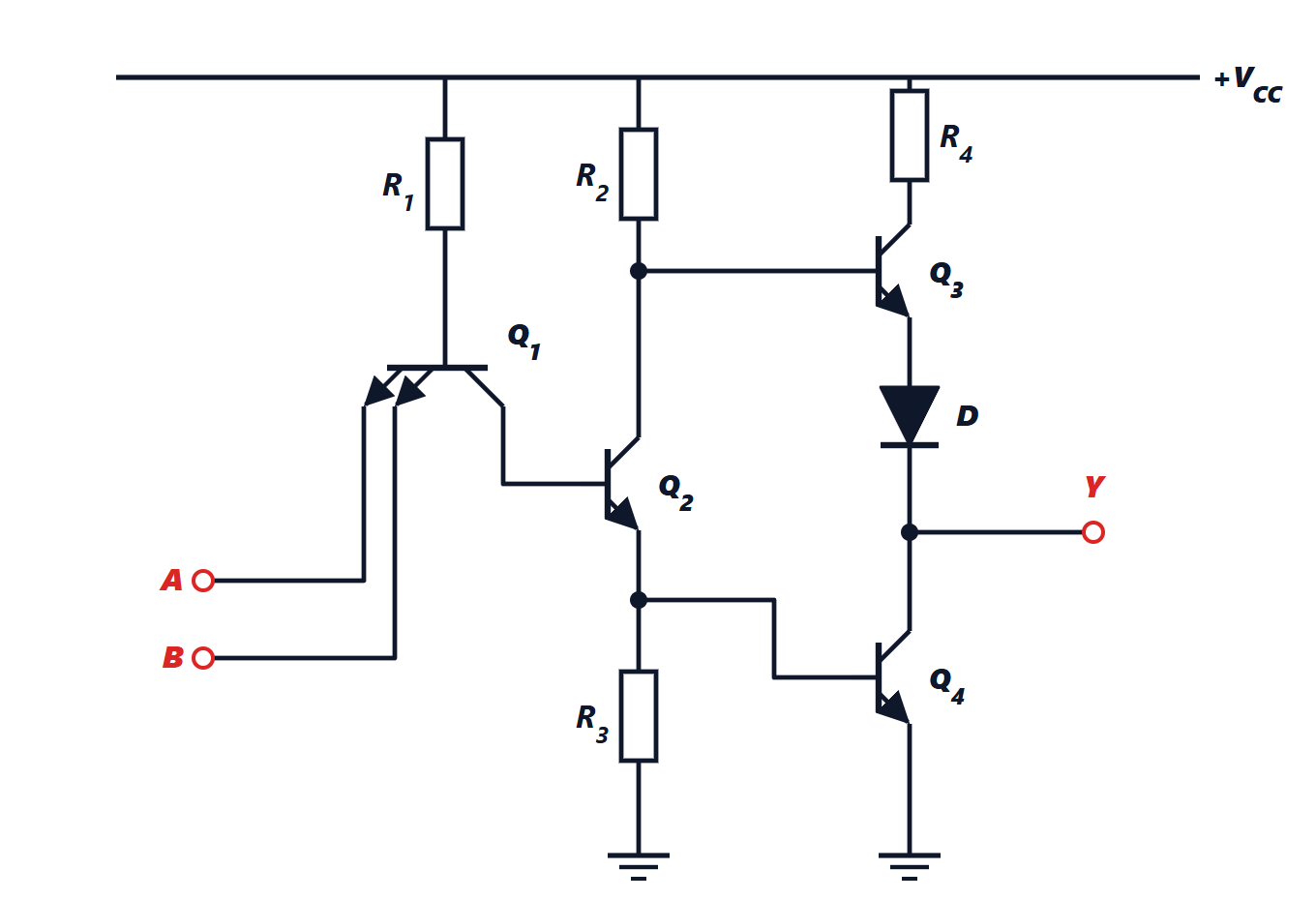
Transistor-Transistor Logic replaces the input diodes with a multi-emitter transistor (Q1) and adds an active output stage. It is worth following it state by state.
One input low (0.2 V). The base-emitter junction of Q1 on that input conducts: the base of Q1 sits at 0.9 V and  mA flows out of R1 and leaves the gate through the input (this is the current
 that the driver must sink). Q1 is saturated and holds the base of Q2 at about 0.3 V: Q2 and Q4 are off. R2 pulls the base of Q3 towards the supply, and Q3 with diode D pulls the output up:
 V.
All inputs high. The input junctions of Q1 are reverse biased; the current of R1 flows through the base-collector junction of Q1 (which works “backwards”) into the base of Q2. Q2 saturates, its emitter current turns Q4 on, which saturates and pulls the output to  between 0.1 and 0.3 V.
Theorem. With the output low, diode D guarantees that Q3 is off.
Proof. The base of Q3 is the collector of the saturated Q2:  V. For Q3 to conduct its base would have to be at least at
 V. Since 0.9 V < 1.6 V, Q3 is cut off. Without the diode the threshold would be
 V, exactly equal to the base voltage: Q3 would conduct and a current limited only by R4 would flow from the supply to ground through Q3 and Q4. ∎
The totem-pole stage. At the top an emitter follower (Q3), at the bottom a saturated switch (Q4): the output has low resistance in both states. This is the great advantage of TTL: load capacitances are charged and discharged quickly in both directions, whereas in RTL and DTL the rising edge goes through a resistor.

The transfer characteristic (figure, left) has three segments. Up to about 0.6 V Q2 is off and the output is high. Between 0.6 and 1.4 V Q2 conducts in the active region but Q4 is still off: Q2 is a common-emitter amplifier with a gain of about  (SPICE gives −1.44, with the follower Q3 and the load). At about 1.4 V, when the voltage on the emitter of Q2 reaches the of Q4, Q4 turns on and the output collapses. The logic threshold (where the output crosses 1.5 V) is at 1.43 V.
The current spike (figure, right). During switching Q3 and Q4 conduct together for an instant, and a current limited only by R4 = 130 Ω flows from the supply to ground: in the simulation 16.5 mA, five times the quiescent current. At every transition, therefore, each gate asks the supply for a current pulse a few nanoseconds long. This is why in TTL circuits a 100 nF decoupling capacitor is placed next to every IC.
Guaranteed levels. The 74 series data sheet guarantees  V,
 V, and that an input is read high above
 V and low below
 V. The guaranteed noise margins are therefore
 V and
 V. Typical values are better: in the simulation the high output is at 3.61 V and the low one at 0.31 V, and with 0.8 V at the input the output is still at 3.28 V, well above the guaranteed 2.4 V.
Fan-out. A low output is guaranteed to sink  mA, and each low input supplies at most
 mA (the worst-case value, with tolerances; in the simulation 1.05 mA); a high output supplies 400 µA and each high input draws at most 40 µA. In both cases the ratio is 10: fan-out of 10.
Speed and power. With ten loads and 15 pF the simulation gives delays of 9.2 ns (output falling) and 7.6 ns (output rising), of the same order as the 10 ns of the data sheet. The supply current is 1.4 mA with the output high and 3.1 mA with the output low: on average 11 mW per gate. The delay-power product (the energy spent per transition, a figure of merit of the technology) is about 100 pJ.
Special outputs. Two totem-pole outputs cannot be connected together: if one pulls up and the other down, a destructive current flows. For buses there are open-collector outputs (without Q3, with a common external pull-up resistor: connected outputs form a wired AND) and tri-state outputs (an enable input turns off both Q3 and Q4, and the output becomes an open circuit).
Schottky TTL
The saturated TTL transistor must get rid of its stored charge before turning off. The solution is a Schottky diode between base and collector: it conducts at 0.3 to 0.4 V, less than the base-collector junction, and diverts the excess base current into the collector before the transistor saturates. The transistor stays at the edge of the active region and turns off immediately. The 74S series has delays of 3 ns (at 19 mW), the 74LS (Low-power Schottky) delays similar to the standard 74 with one fifth of the power, 2 mW: a delay-power product of 19 pJ, five times better. The 74LS was the basic logic of electronic boards for twenty years; the 74ALS and 74F followed.
ECL
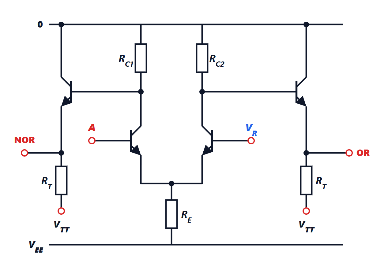
Emitter-Coupled Logic is built around a differential pair. The current set by  flows either in the input transistor or in the reference one, depending on whether the input is above or below
 V: it is a current switch. The output followers restore the right levels to drive other gates, and together provide the two complementary OR and NOR outputs. Values of the 10K series:
 V, ground as the positive supply (so that supply noise reaches the outputs less),
 Ω,
 Ω,
 Ω, outputs on 50 Ω resistors to
 V, which are also the termination of the transmission lines.
The levels. With the input low the reference transistor conducts: the common emitter sits at  V and the current is
 mA. The OR output (from the right collector) is low:
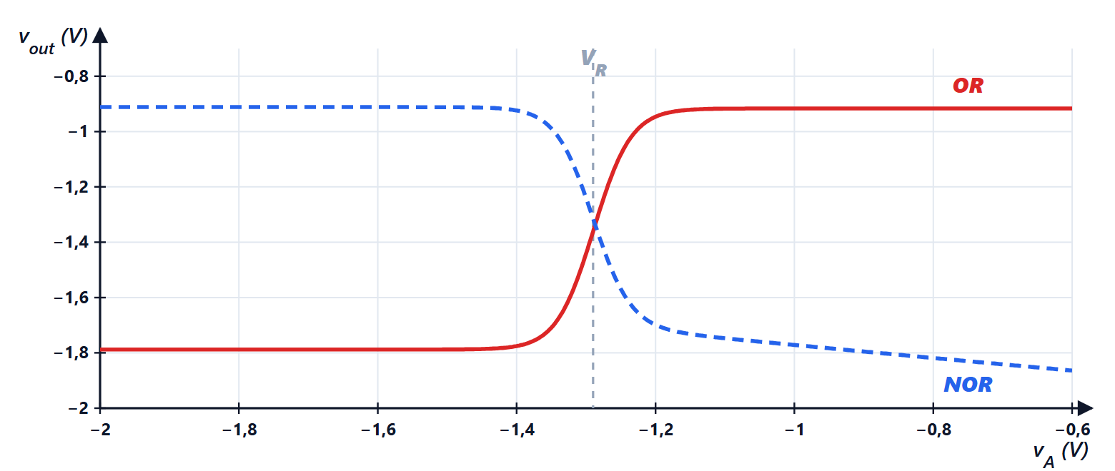
 V. The high output is one below ground: about −0.9 V. The simulation gives −0.91 and −1.79 V, with the unity-slope points at
 V and
 V: noise margins of 0.29 V (high) and 0.41 V (low). The logic swing is only 0.9 V.
Theorem. In the ECL gate no transistor of the pair saturates.
Proof. The base of the input transistor is at most at  V. Its collector falls at most by
 , with
 mA (SPICE: 4.9 mA with the complete model), that is, down to about −1.0/−1.1 V. The base-collector junction is therefore at most slightly forward biased, by 0.1 to 0.2 V, much less than the roughly 0.5 V needed for it to conduct: the transistor stays in the active region. The same holds for the reference transistor, whose base is fixed at −1.29 V and whose collector does not go below −1.0 V. ∎
Not saturating, and with small swings, ECL is the fastest bipolar family: delays of 2 ns for the 10K series and less than one nanosecond for the 100K (in the simulation without load, 0.5 and 0.6 ns). The price is power: the pair draws 4 mA from 5.2 V (21 mW) and the output terminations as much again, always, even when idle. ECL was used in supercomputers (Cray) and mainframes; today the same idea survives in the CML (Current-Mode Logic) of serial links at tens of gigabits per second.
The comparison
| family | typical delay | power per gate | delay × power |
|---|---|---|---|
| RTL | 12 ns | 12 mW | 140 pJ |
| DTL | 30 ns | 8 mW | 240 pJ |
| TTL 74 | 10 ns | 10 mW | 100 pJ |
| TTL 74S | 3 ns | 19 mW | 57 pJ |
| TTL 74LS | 9.5 ns | 2 mW | 19 pJ |
| ECL 10K | 2 ns | 25 mW | 50 pJ |
| CMOS 74HC | 8 ns | almost zero when idle | depends on the frequency |
The bipolar families consume power even when idle, because in one of the two states there is always a current flowing in a resistor. CMOS (lesson on CMOS logic) consumes power only when switching, to charge the capacitances, and has noise margins close to half the supply; with scaling it also became faster. This is why it replaced almost all bipolar logic. What remains is ECL/CML for extreme speeds and BiCMOS, which combines bipolar and MOS transistors on the same chip.
Summary
- In logic gates the transistor is a switch between cut-off and saturation; saturation slows down turn-off because of the stored charge.
- RTL: NOR with base resistors; the high level falls with fan-out (0.94 V with ten loads).
- DTL: NAND with diodes, higher threshold and a high level independent of fan-out.
- TTL 7400: multi-emitter transistor, phase splitter and totem-pole output; guaranteed levels 2.4/0.4 V at the output and 2.0/0.8 V at the input, 0.4 V margins, fan-out 10, 10 ns and 10 mW; diode D keeps Q3 off with the output low; the switching current spike requires decoupling capacitors.
- Schottky: a base-collector diode prevents saturation (74S fast, 74LS low power).
- ECL: a current switch that never saturates, levels −0.9/−1.8 V, the fastest and the most power-hungry.
The code
# BJT logic gates: hand calculations of levels, fan-out and noise margins

# RTL (VCC 3.6 V, RB 450, RC 640): high output loaded by N inputs in parallel
VCC, RB, RC, VBE, VCEsat, beta = 3.6, 450.0, 640.0, 0.75, 0.1, 50
for N in (1, 2, 5, 10):
    # the collector resistor and the N base resistors in parallel form a divider towards VBE
    VOH = VBE + (VCC - VBE) * (RB / N) / (RB / N + RC)
    IB = (VOH - VBE) / RB                       # base current of each load
    sat = beta * IB > (VCC - VCEsat) / RC       # the load saturates if beta IB exceeds the saturation current
    print(f"RTL, N = {N:2d}: VOH = {VOH:.2f} V, high margin {VOH - VBE:.2f} V, loads saturated: {sat}")

# TTL 7400 (VCC 5 V): low input current, high level, fan-out and guaranteed margins
VCC, R1 = 5.0, 4e3
IIL = (VCC - (0.2 + 0.7)) / R1                  # input at 0.2 V: the base of Q1 sits 0.7 V above
print(f"TTL: low input current {1e3 * IIL:.2f} mA, unloaded high output about {VCC - 0.7 - 0.7:.1f} V")
IOL, IILmax, IOH, IIHmax = 16e-3, 1.6e-3, 0.4e-3, 40e-6
print(f"TTL: fan-out = min({IOL / IILmax:.0f}, {IOH / IIHmax:.0f})")
VOL, VOH, VIL, VIH = 0.4, 2.4, 0.8, 2.0
print(f"TTL: guaranteed margins NML = {VIL - VOL:.1f} V, NMH = {VOH - VIH:.1f} V")
# from the simulation: typical levels and thresholds where the slope is -1
vol, voh, vil, vih = 0.31, 3.61, 0.59, 1.50
print(f"TTL simulated with fan-out 10: NML = {vil - vol:.2f} V, NMH = {voh - vih:.2f} V")
icch, iccl, tp = 1.40e-3, 3.14e-3, 8.4e-9
P = VCC * (icch + iccl) / 2
print(f"TTL: mean power {1e3 * P:.1f} mW, power-delay product {1e12 * P * tp:.0f} pJ")

# ECL (VEE -5.2 V, reference -1.29 V, RE 779, RC 220/245): tail current and levels
VEE, VR, RE, RC2, VBEf = -5.2, -1.29, 779.0, 245.0, 0.8
I = (VR - 0.75 - VEE) / RE
print(f"ECL: tail current {1e3 * I:.2f} mA, VOL = {-I * RC2 - VBEf:.2f} V, VOH about {-VBEf - 0.1:.2f} V")
print(f"ECL: gate power {1e3 * abs(VEE) * I:.0f} mW, plus the output terminations")
The program prints the RTL table (1.93, 1.49, 1.10 and 0.94 V), the TTL input current (1.02 mA), the fan-out of 10, the guaranteed margins (0.4 V) and those of the simulation (0.28 and 2.11 V, measured however at the slope −1 points, a stricter criterion than the data sheet’s), the mean power of 11.3 mW with a product of 95 pJ, and for ECL the current of 4.06 mA with the low level at −1.79 V.
The ngspice netlist of the TTL NAND, with the output loaded by ten identical gates:
* TTL 7400 NAND: transfer characteristic and delays with fan-out 10
.subckt nand a bb out vcc
R1 vcc b1 4k
Q1a c1 b1 a QN
Q1b c1 b1 bb QN
R2 vcc c2 1.6k
Q2 c2 c1 e2 QN
R3 e2 0 1k
R4 vcc c3 130
Q3 c3 c2 e3 QN
D1 e3 out DN
Q4 out e2 0 QN
.ends
VCC vcc 0 5
VCC0 vcc0 0 5
VA a 0 dc 0 pulse(0.2 3.4 20n 3n 3n 60n 120n)
X0 a vcc out vcc0 nand
X1 out vcc o1 vcc nand
X2 out vcc o2 vcc nand
X3 out vcc o3 vcc nand
X4 out vcc o4 vcc nand
X5 out vcc o5 vcc nand
X6 out vcc o6 vcc nand
X7 out vcc o7 vcc nand
X8 out vcc o8 vcc nand
X9 out vcc o9 vcc nand
X10 out vcc o10 vcc nand
CL out 0 15p
.model QN NPN(IS=1e-15 BF=50 BR=0.1 VAF=50 RB=50 RC=20 CJE=1.5p CJC=1p CJS=2p TF=0.25n TR=15n)
.model DN D(IS=1e-15 CJO=1p RS=10)
.control
dc VA 0 2.5 0.005
let dv = deriv(v(out))
meas dc vil when dv=-1 fall=1
meas dc vih when dv=-1 rise=1
meas dc vt when v(out)=1.5 fall=1
let icc = -i(vcc0)
meas dc icc_pk max icc
tran 0.05n 200n
meas tran tphl trig v(a) val=1.5 rise=1 targ v(out) val=1.5 fall=1
meas tran tplh trig v(a) val=1.5 fall=1 targ v(out) val=1.5 rise=1
.endc
.end
It prints the slope −1 points (0.59 and 1.50 V), the threshold of 1.43 V, the current peak of 16.5 mA and the delays of 9.2 and 7.6 ns.


Benvenuti nella pagina su «Porte logiche a BJT: RTL, DTL, TTL 7400, Schottky ed ECL». L'ho scritta pensando a chi studia ingegneria elettronica: se un passaggio non vi torna, un esercizio vi dà un risultato diverso o volete altro materiale sull'argomento, chiedete pure nei commenti e vi risponderò. Un voto con le stelle qui sopra mi aiuta a capire quali pagine migliorare.Welcome to the page on “BJT logic gates: RTL, DTL, TTL 7400, Schottky and ECL”. I wrote it for engineering students: if a step does not add up, an exercise gives you a different result or you would like more material on the topic, just ask in the comments and I will reply. A star rating above helps me understand which pages to improve.