Logic levels, noise margins, delays and output types
VOH, VOL, VIH, VIL voltages, noise margins with an example, level shifters, propagation delay and fan-out, power, push-pull, open-drain and three-state outputs, floating inputs.
For Boolean algebra a signal is 0 or 1; for electronics it is a voltage, never exactly 0 or  , disturbed by noise, by drops along traces and by coupling with nearby lines. For a digital circuit to work you need to know which voltages are recognised as 0 and as 1, how much disturbance can be tolerated and how long a gate takes to respond. In this lesson we cover logic levels, noise margins, delays, power and the different kinds of output.
Logic levels
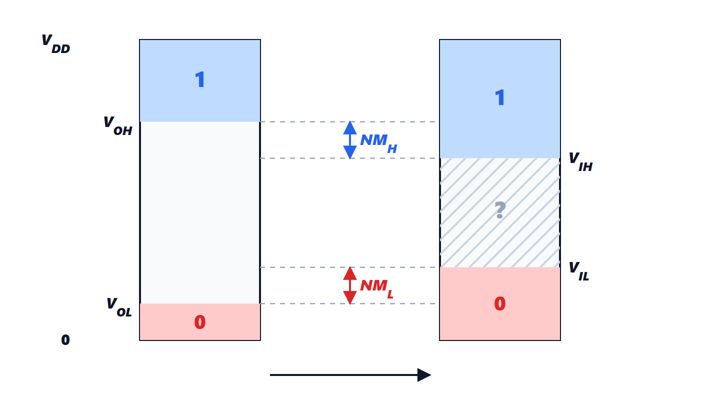
Every logic family specifies four voltages:
 : the minimum voltage an output guarantees when high;
 : the maximum voltage an output guarantees when low;
 : the minimum voltage an input surely recognises as 1;
 : the maximum voltage an input surely recognises as 0.
Between and is a forbidden zone: there the input may read anything, and a signal lingering there also makes both transistors of the CMOS input conduct, with abnormal current draw.
Noise margins

They are the largest disturbances that can be added to the signal without the next gate misreading it.
Example. For typical 3.3 V LVCMOS logic, with  V,
 V,
 V and
 V:
 V. A long trace picking up 0.5 V of disturbance from a nearby line is already out of specification.
Connecting different families. A 3.3 V output driving a 5 V input with  V is not safe: 3.3 V is below the threshold. Conversely a 5 V output can damage a 3.3 V input that is not tolerant. Level shifters are needed: dedicated chips, or a MOSFET with pull-up resistors for slow buses such as I²C.
Delays
A gate does not switch instantly. The propagation delay  is the time between the input crossing 50% of its swing and the output doing so;
 and
 are distinguished for the two transitions. The rise and fall times (between 10% and 90%) say how steep the edges are. As seen in the CMOS lesson, the delay is about
 : it grows with the capacitance to be driven, that is with the number of inputs connected to the output (fan-out) and with trace length.
In modern integrated circuits gate delays are tens of picoseconds, and the interconnect often dominates: a long wire on the chip is a distributed RC line whose delay grows with the square of its length. That is why buffers are inserted along long connections.
Power
The power of a CMOS gate is almost entirely dynamic,  (proof in the CMOS logic lesson), plus a small static part due to leakage currents. Lowering the voltage is the most effective way to reduce power, which is why logic has moved from 5 V to 3.3, 1.8 V and below. Other techniques: stopping the clock of idle blocks (clock gating), cutting the supply of blocks that are off (power gating), lowering voltage and frequency when less computing power is needed.
Kinds of output
- Totem pole (push-pull): the normal CMOS output, which actively drives the line both to 0 and to 1. Two push-pull outputs tied together trying to force different values create a short circuit.
- Open drain (or open collector): the output can only pull the line to 0; an external pull-up resistor brings it to 1. Several outputs can share the same line: one going to 0 is enough to make the line 0 (a “wired” AND). This is the principle of the I²C bus and of shared interrupt lines. The price is a slow rising edge, set by the pull-up and the line capacitance.
- Three-state (tri-state): besides 0 and 1, the output can be disconnected (high impedance). Many outputs share a bus, and an enable signal decides who talks; the others must be in high impedance.
Inputs not to forget
A CMOS input left unconnected is neither 0 nor 1: it charges randomly and can oscillate, draw current and make the logic toggle. Every unused input must be tied to ground or to the supply, directly or through a resistor. Push-buttons need a pull-up or pull-down, and produce bounce (dozens of transitions in the first milliseconds), removed with a Schmitt trigger and an RC filter or in software.