Magnetic components and thermal design
The gapped inductor with inductance proved, the saturation check, Steinmetz losses, skin effect and Litz wire, the thermal circuit and heatsink selection with an example, Arrhenius and thermal cycling.
In a converter the largest, heaviest and often most expensive components are the inductors and transformers, and the power limit of any device is the heat it can get rid of. The design of magnetic components and thermal design therefore decide size, efficiency and lifetime. In this lesson we look at the gapped inductor with the proof of its inductance, the saturation check, core and winding losses, the equivalent thermal circuit with an example of heatsink selection, and the link between temperature and reliability.
The gapped inductor
A power inductor is a winding of  turns on a ferrite or powdered-metal core, with a small air gap, a space of length
 in the magnetic circuit.
Theorem. If the core permeability is much greater than that of air, the inductance is
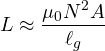
where  is the core cross-section: it depends on the gap, not on the material.
Proof. By Ampère’s law along the magnetic circuit,  , with
 and
 the field and length in the core,
 and in the gap. The flux
 is the same in the core and in the gap, so
 and
 . If
 is large,
 and
 , i.e.
 . The flux linkage is
 , and the inductance is
 . ∎
The gap looks like a waste, but it is essential: it makes the inductance stable (independent of the material’s permeability, which varies with temperature and from piece to piece), and almost all the energy  is stored precisely in the gap’s volume of air, where the field
 is large. A core without a gap would saturate with tiny currents.
Saturation
Every magnetic material has a saturation flux density  , about 0.3-0.4 T for ferrites and 1-1.5 T for iron powders: beyond it, permeability collapses, the inductance vanishes and the current explodes. The design must check that at peak current the flux density stays below the limit. From the previous proof,
 , so
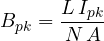
For a given inductance and current, the product  must be large enough: that is why an inductor that must carry more current is bigger. In converters the peak current includes ripple and transients: a buck that goes into short circuit drives the inductor into saturation if the protection is not fast enough.
Losses
- In the core: hysteresis and eddy currents dissipate energy every cycle. They are estimated with the empirical Steinmetz law,
 per unit volume, with
 between 1 and 2 and
 between 2 and 3, from the manufacturer’s data. What matters is the amplitude of the field ripple, not its mean value.
- In the windings: besides the DC resistance, at high frequencies the current concentrates on the conductor’s surface because of the skin effect (Electromagnetic Fields lesson on waves): at 100 kHz the skin depth in copper is about 0.2 mm, and a thick wire is almost useless. Litz wire, made of many thin insulated strands twisted together, or foil and printed windings are used. Between adjacent layers there is also the proximity effect, which can multiply the losses.
The thermal circuit
The heat produced in a semiconductor must cross the package, the interface (thermal paste or pad) and the heatsink before reaching the air. Like a current in a series of resistances, the thermal power  produces temperature drops proportional to the thermal resistances (Technical Physics lesson on conduction).
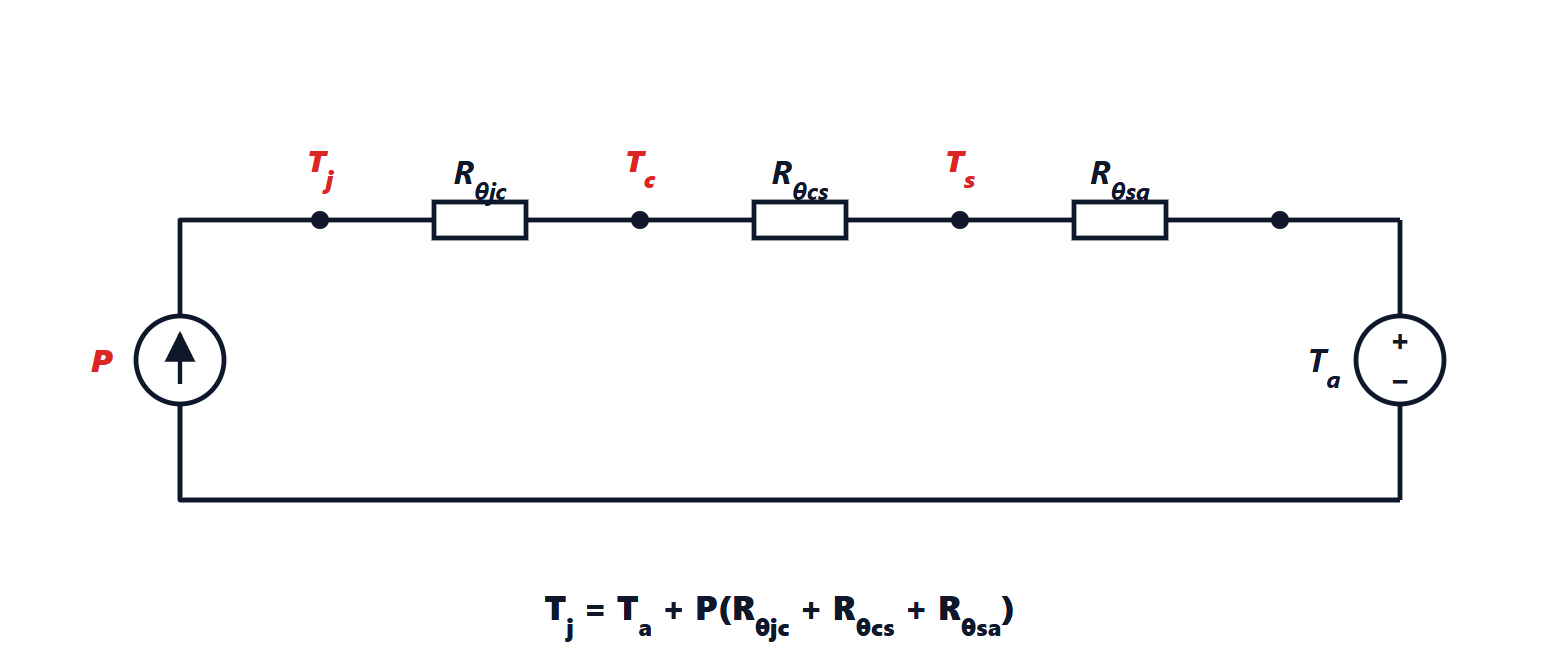

Example. A MOSFET dissipates 20 W, with  K/W and a 0.3 K/W interface. The junction must not exceed 150 °C, and a margin is advisable: aim for 125 °C, with air at 40 °C. The available rise is 85 K, which divided by 20 W gives 4.25 K/W in all; subtracting 0.8 K/W for junction and interface, the heatsink must have
 K/W. With forced air a heatsink of the same size has a thermal resistance two to five times lower.
For short pulses the transient thermal impedance matters: the heat first warms the mass of the chip and only later reaches the heatsink, and a device can withstand for a few milliseconds a power much greater than the continuous one. Manufacturers give the curves.
Temperature and reliability
Many failure mechanisms (diffusion, electromigration, electrolyte degradation in capacitors) accelerate with temperature according to the Arrhenius law: as a rule of thumb, every 10 °C more halves the lifetime. In electrolytic capacitors, often the most fragile components of a power supply, a rated life of a few thousand hours at 105 °C becomes tens of thousands at 65 °C. Thermal cycling matters too: repeated expansion between different materials fatigues solder joints and the internal bond wires of power modules, and is the main cause of failure in car and wind-turbine inverters. That is why serious designs leave temperature margins and modern modules use assembly techniques such as silver sintering.