Delays in integrated circuits: Elmore and logical effort
The Elmore delay of RC networks, logical and electrical effort, the minimum delay of a path proved with the geometric mean, the optimal number of stages, an inverter chain.
How fast is a logic gate, and how should the transistors be sized to drive a large load in the shortest time? Simulations give precise answers, but design needs simple models that point in the right direction. In this lesson we look at the Elmore delay of RC networks, the logical effort model of gate delay, the proof of how to minimise the delay of a path by sharing the effort equally, and an example with a chain of inverters.
The Elmore delay
A switching gate charges or discharges the downstream capacitances through the resistance of its transistors and interconnects: an RC network. For a tree network driven by a step, a widely used estimate of the delay to node  is the Elmore delay
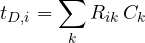
where the sum runs over all the capacitances  of the network and
 is the resistance of the portion of path shared between the path from the source to node and that from the source to node
 . For a chain of
 segments, with resistances
 and capacitances
 , it becomes
 : each capacitance is charged through all the resistances preceding it.
The idea is that each capacitance, to charge, passes its charge through the resistances it shares with the observed path, and each produces a drop there that delays the node. Mathematically the Elmore delay is the first moment of the network’s impulse response, and it is an upper bound on the 50 % delay: imprecise in the details, but simple, additive and almost always in the right direction, perfect for comparing alternatives.
The logical effort model
The delay of a gate, measured in units of  (the delay of an ideal inverter driving an identical inverter), is written

 is the electrical effort (electrical fan-out): how much load it drives relative to its own input capacitance;
 is the logical effort: how much worse the gate is than an inverter at producing current for the same input capacitance. It is 1 for the inverter, 4/3 for a two-input NAND, 5/3 for a two-input NOR, because series transistors must be widened to give the same current;
 is the parasitic delay, due to the output’s own capacitance: about 1 for the inverter, 2 for the two-input NAND.
The product  is the stage effort.
The minimum delay of a path
For a path of stages the path effort is defined as  , the product of the total logical effort
 , the total electrical effort
 and a branching factor
 .
 does not depend on how the intermediate gates are sized: it is fixed by the final load, the allowed input capacitance and the logic.
Theorem. The delay of an -stage path with path effort is minimum when all stages have the same effort

and it is then  .
Proof. The delay is  , and the second term does not depend on sizing. The product of the stage efforts is fixed:
 , because the intermediate loads cancel between one stage and the next. By the inequality between arithmetic and geometric means,
 , with equality only if all the
 are equal. So
 is minimum, equal to
 , when each stage has effort
 . ∎
The number of stages can also be chosen: minimising  with respect to one finds that the optimal stage effort is about 3.6, in practice between 3 and 5. Adding inverters to a path that is too short makes it faster, and so does removing them from one that is too long.
An example
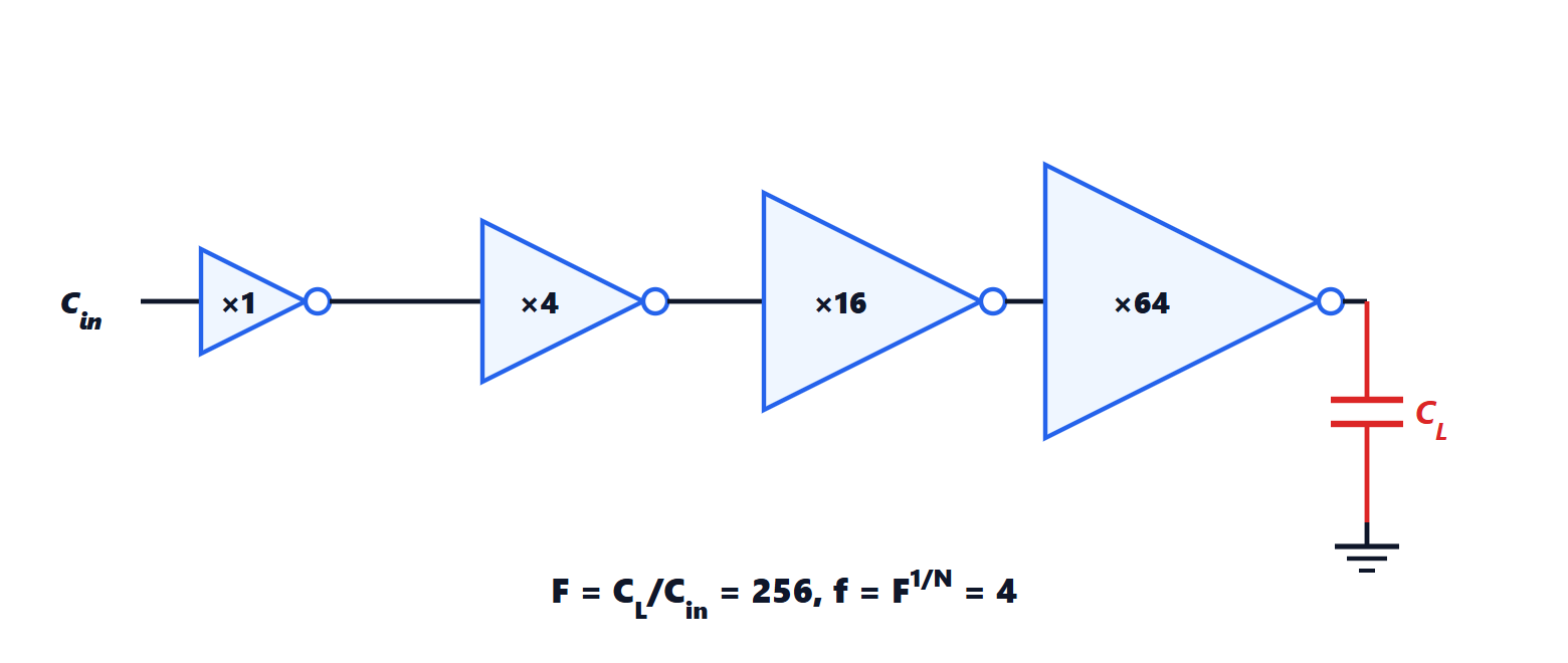
A signal with input capacitance  must drive a load
 , for instance a long bus or an output pad. With a single inverter the delay is
 . With a chain of inverters the path effort is
 ; with
 stages the optimal effort of each is
 , and each inverter must be four times larger than the previous one: 1, 4, 16, 64. The total delay is
 , almost thirteen times less. That is why output buffers and clock drivers are chains of progressively larger inverters, and why an experienced designer, looking at a critical path, first looks for stages whose effort is very different from the others.