Noise and mismatch in integrated analogue circuits
kT/C noise proved and the energy cost of precision, thermal and flicker noise of MOSFETs, Pelgrom's law with justification and example, common centroid and layout techniques.
In an integrated analogue circuit two random phenomena limit precision: noise, which varies in time, and mismatch, which makes two components drawn identically different, and stays fixed. Both are fought with the same currency: area and power. In this lesson we look at the thermal noise of a sampler with the proof of the kT/C result and its energy cost, transistor noise, Pelgrom’s law for mismatch with its justification, and the layout techniques that reduce systematic errors.
kT/C noise
Every circuit that samples a voltage onto a capacitor (analogue-to-digital converters, switched-capacitor filters) uses a switch, a transistor with an on-resistance  . The thermal noise of this resistance (Signal Theory lesson on random processes) reaches the capacitor, and when the switch opens the instantaneous value of the noise is frozen together with the signal.
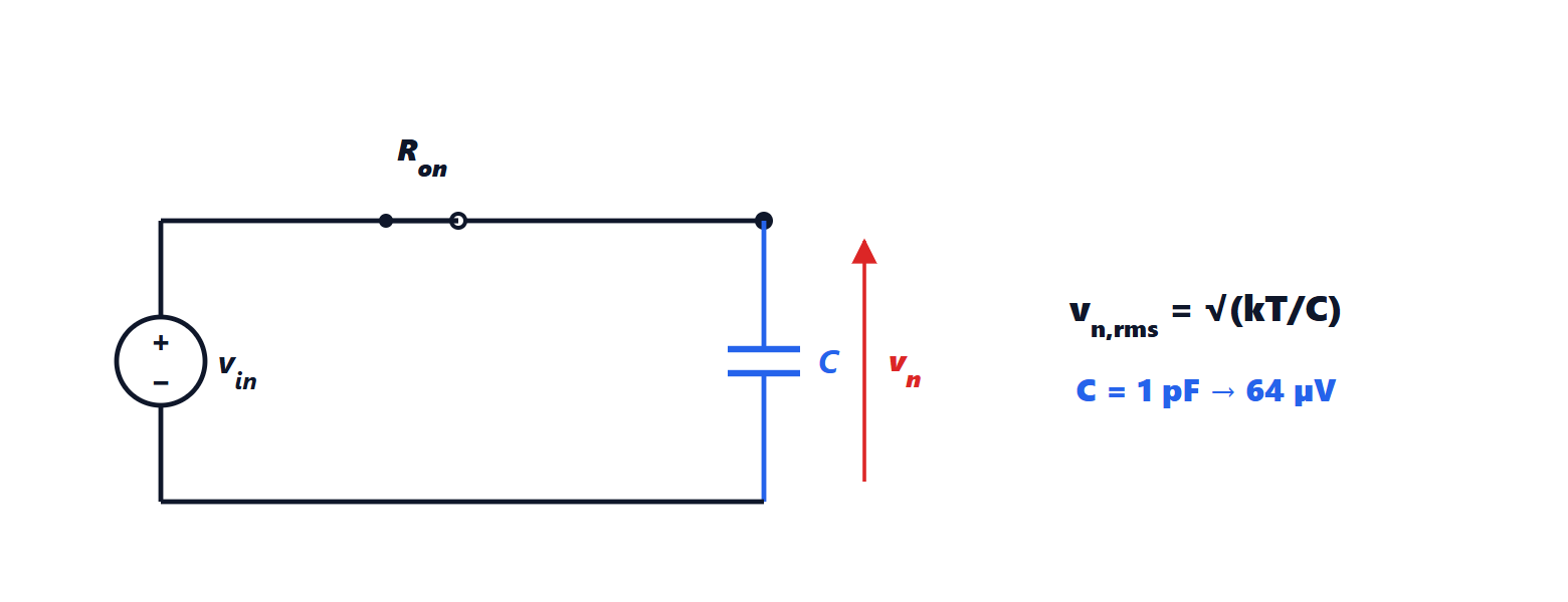
Theorem. The RMS noise voltage on the capacitor is
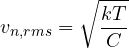
regardless of the value of the resistance.
Proof. The resistance has a noise voltage spectral density  (in V²/Hz). This noise passes through the RC low-pass filter, with
 . The variance of the voltage on the capacitor is the integral over all frequencies:

using  with
 . The resistance cancels: a larger resistance makes more noise, but over a narrower bandwidth. ∎
Example. With  pF at 300 K:
 µV. A 12-bit converter with 1 V full scale has a 244 µV step, and kT/C noise is acceptable; for 16 bits (15 µV step) a capacitor of tens of picofarads would be needed.
The consequence is a direct link between precision and energy: halving the noise requires a capacitor four times larger, and charging it at the same speed requires four times the current. Every extra bit of resolution in a converter limited by thermal noise costs about four times the energy per conversion.
Transistor noise
- The thermal noise of a MOSFET channel in saturation is represented as a current of density
 , with
 between 2/3 and 1 and above in short transistors. Referred to the input it is a voltage of density
 : reducing it requires a large transconductance, i.e. current.
- Flicker (1/f) noise, due to the trapping and release of charges in oxide traps, has a density that grows as frequency decreases and is inversely proportional to the gate area. It dominates at low frequencies, below the corner frequency, which ranges from kilohertz to megahertz. It is reduced with large transistors, or eliminated with chopper and auto-zero techniques, which move the signal to a higher frequency before amplifying it and bring it back afterwards.
Mismatch
Two transistors drawn identically and close together are not equal: threshold voltage and current factor differ by a random amount (lesson on the nanometre MOSFET). In a current mirror or a differential pair this produces current errors and offset voltages.
Pelgrom’s law. The standard deviation of the threshold difference between two identical transistors is
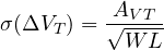
where  is a process constant, typically a few mV·µm.
Justification. The threshold depends on the number of fixed charges (dopant atoms, charges in the oxide) under the gate. These are distributed randomly and independently: their number in an area  has a mean proportional to the area and, as for a Poisson distribution, a standard deviation proportional to the square root of the area. The threshold is proportional to the charge density, i.e. the number divided by the area: its relative fluctuation goes as
 . The difference between two independent transistors has a standard deviation
 times that of one, absorbed into the constant. ∎
Example. With  mV·µm, a 1 µm × 1 µm input pair has
 mV, and 99.7 % of circuits have an offset within ±9 mV. To get down to a 1 mV standard deviation transistors nine times larger are needed, with more capacitance and hence less speed. Precision amplifiers therefore use trimming after production or auto-zero techniques.
Layout for matching
Besides random errors there are systematic errors: doping, thickness and temperature gradients across the chip, mechanical stress from the package. Layout cancels them with a few rules:
- common centroid: the transistors to be matched are split into parts arranged symmetrically around the same centre (for instance ABBA, or a checkerboard), so that a linear gradient affects them equally;
- interdigitation of the transistors’ fingers;
- dummy devices at the edges of arrays, because edge devices see a different environment during lithography and etching;
- same orientation, distance from heat sources and from the corners of the chip, where stress is greatest.