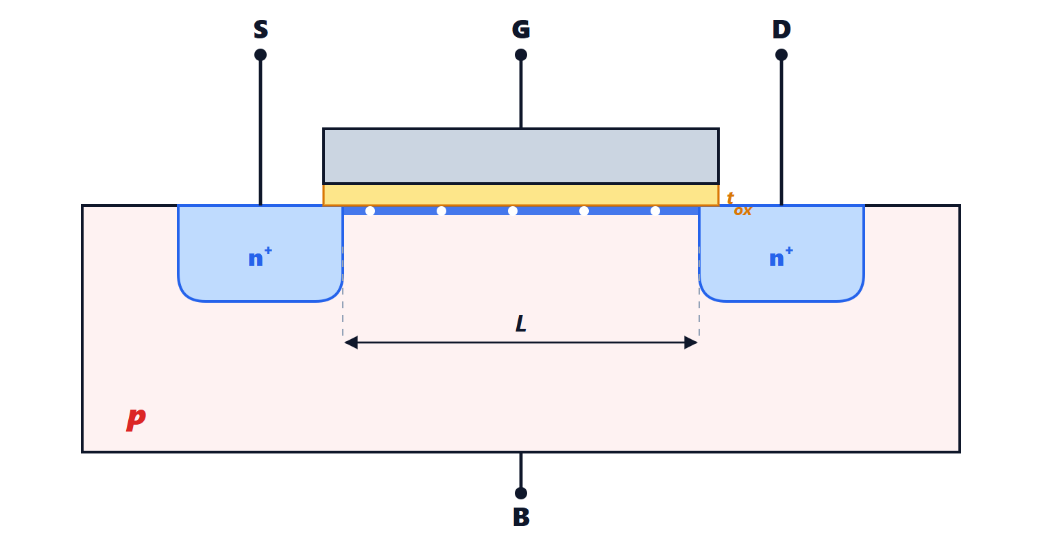
Transport in semiconductors: drift, diffusion and recombination
Mobility and drift current, resistivity, diffusion and Fick's law, the Einstein relation with proof, lifetime, LEDs, the continuity equation and diffusion length.
Knowing how many carriers there are is not enough: to compute a current you need to know how they move. In a semiconductor they move in two ways: pulled by an electric field (drift) or pushed by a concentration difference (diffusion). How diodes and transistors work comes down to the competition between these two mechanisms and recombination.
Drift current
A free electron in a field  accelerates but keeps colliding with the vibrating lattice and with impurities: on average it reaches a drift velocity proportional to the field,

where  is the mobility. In lightly doped silicon
 cm²/(V·s) and
 cm²/(V·s): holes are almost three times slower, which is one reason circuits favour n-channel transistors. The total current density is

which is Ohm’s law in local form, with conductivity  .
Example. Intrinsic silicon:  Ω·cm. With
 cm⁻³:
 Ω·cm, almost a million times lower. Copper has
 Ω·cm.
At high fields (above about  V/cm) the velocity stops growing and saturates at about
 cm/s: this is what limits the speed of the smallest transistors.
Diffusion current
If carriers are more concentrated on one side, their random motion takes them on average towards the less concentrated region, like a drop of ink in water. The flux is proportional to the gradient (Fick’s law):

 is the diffusion coefficient. The signs differ because the charges are opposite: electrons and holes both diffuse towards lower concentration, but the hole current flows in the direction of their motion, the electron current in the opposite direction.
The Einstein relation
Mobility and diffusion are not independent: both depend on collisions with the lattice.
Theorem (Einstein relation).
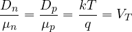
Proof. Consider a semiconductor at equilibrium with non-uniform doping. Electrons diffuse and set up a field  , and at equilibrium the total electron current is zero:
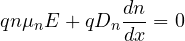
At equilibrium the concentration follows Boltzmann statistics,  (electrons gather where the potential is higher), so
 . Substituting:
 , that is
 . The same reasoning holds for holes. ∎
At 300 K  mV, the thermal voltage, which will appear in every diode and transistor formula. For electrons in silicon
 cm²/s.
Generation, recombination and lifetime
If excess carriers are injected (by light or through a junction), the law  no longer holds and the system returns to equilibrium by recombination. For excess minority carriers
 in n-type material, the recombination rate is
 , where
 is the lifetime: from nanoseconds to milliseconds, depending on the purity of the crystal.
In silicon recombination happens almost always through defects and impurities (levels in the middle of the gap) and releases heat. In direct-gap semiconductors such as gallium arsenide and gallium nitride, instead, electron and hole recombine directly by emitting a photon of energy about  : this is the principle of LEDs and lasers. The colour depends on the gap:
 nm with in eV.
The continuity equation and diffusion length
The balance of minority carriers in a small volume says that their concentration changes because of current flowing in or out and because of recombination:
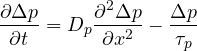
(with no field and no generation). In steady state, with an excess  held at
 , the solution that vanishes far away is

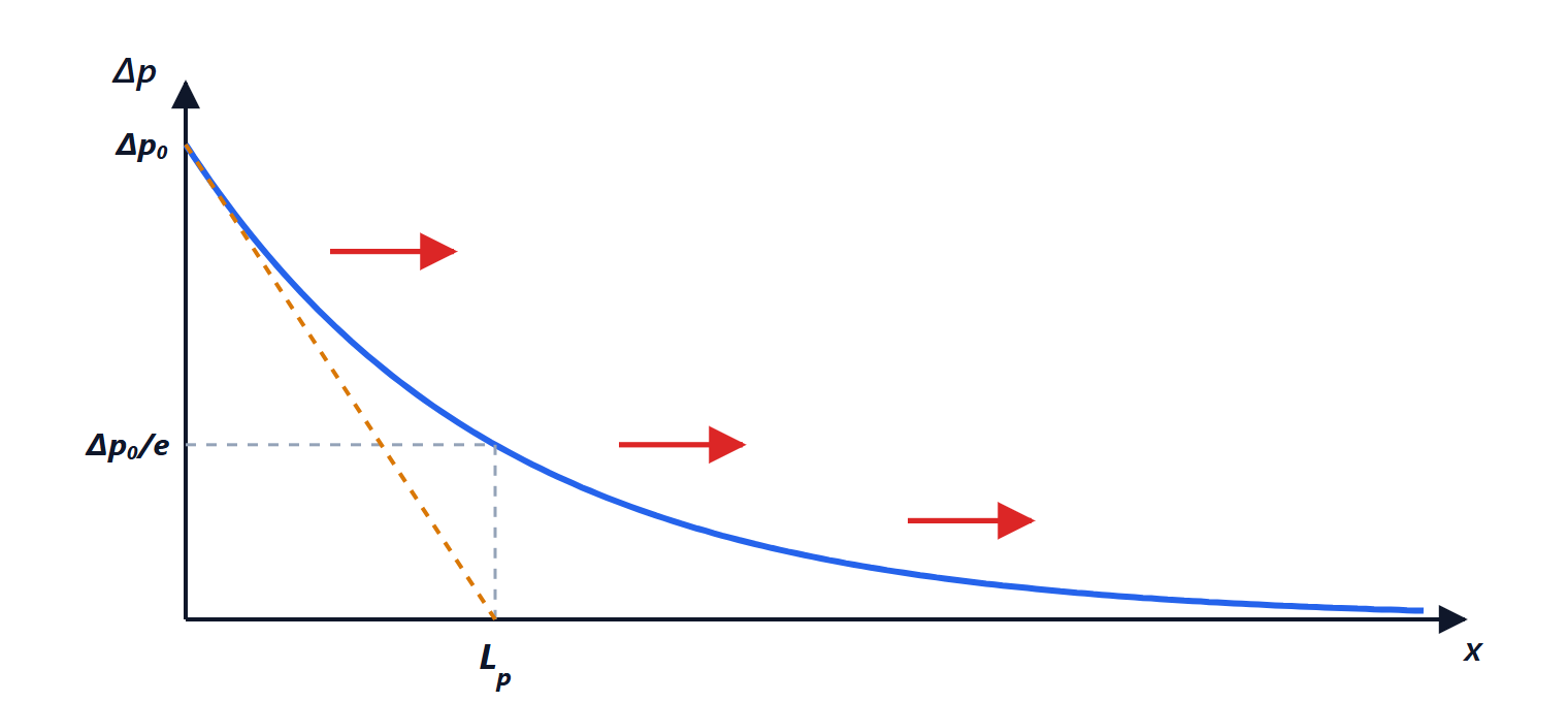
The diffusion length  is the average distance a minority carrier travels before recombining: with
 cm²/s and
 µs,
 µm. This number sets device geometry: in the bipolar transistor the base must be much thinner than
 , so that carriers cross it without getting lost.
The full picture
Putting drift and diffusion together:

These two equations, with the continuity equation and Poisson’s equation for the field, are the model simulators use to compute any semiconductor device. In the next lessons we apply them by hand to the most important cases: the pn junction, the diode, the bipolar transistor and the MOSFET.