Semiconductors: energy bands, electrons and holes, doping
The silicon crystal, electrons and holes, energy bands and the gap, intrinsic concentration, n and p doping, the mass action law with proof, majority and minority carriers.
Diodes, transistors, LEDs, solar cells and microprocessors are nearly all made of the same material: silicon, a semiconductor. Its conductivity lies between that of metals and that of insulators, but above all it can be controlled by adding tiny amounts of other elements. In this lesson we see where the electrons and holes that carry current come from, how doping changes their number and the law linking the two concentrations.
The silicon crystal
Silicon has four valence electrons. In the crystal each atom is bonded to its four neighbours by covalent bonds, each made of two shared electrons. At zero temperature all electrons are tied up in bonds and the crystal is an insulator.
At room temperature thermal agitation occasionally breaks a bond: an electron is freed and can move through the crystal, and the bond is left with an empty place, the hole. An electron from a nearby bond can jump into that empty place, and the hole moves the opposite way. The motion of the hole is equivalent to the motion of a positive charge  : that is why in a semiconductor current is carried by two kinds of carriers, electrons and holes.
Energy bands
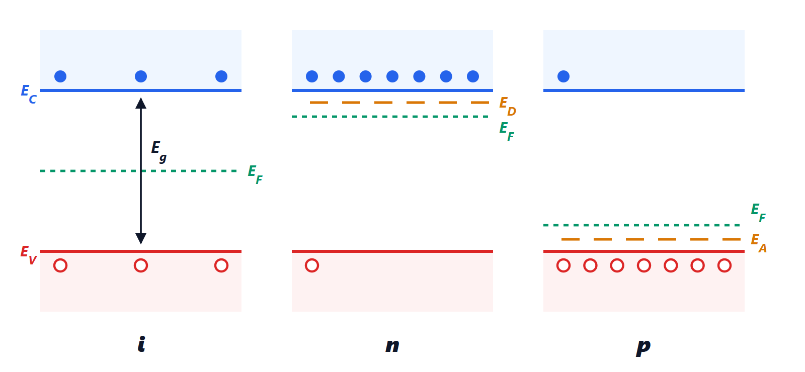
In an isolated atom electrons have discrete energy levels. In a crystal, with about  atoms per cubic centimetre, the levels broaden into bands:
- the valence band, with top energy
 , holds the bonding electrons;
- the conduction band, with bottom energy
 , holds the free electrons;
- between them lies the band gap, of width
 .
In silicon  eV, in germanium 0.66 eV, in gallium arsenide 1.42 eV, in diamond (an insulator) 5.5 eV. In metals the bands overlap and there are always free electrons.
The intrinsic semiconductor
In a pure crystal every freed electron leaves a hole, so the concentrations are equal:  , the intrinsic concentration. It grows quickly with temperature:

where  and
 are material constants (the effective densities of states) and
 at 300 K is 25.9 meV. In silicon at room temperature
 cm⁻³: one free electron every
 atoms. Too few to make a good conductor, and too temperature-dependent to build devices on.
Doping
A small fraction of the silicon atoms is replaced by atoms from another group.
- n-type. A group V atom (phosphorus, arsenic) has five valence electrons: four form the bonds, the fifth is weakly bound (about 0.045 eV for phosphorus) and at room temperature it breaks free. The atom is a donor and becomes a fixed positive ion.
- p-type. A group III atom (boron) has three electrons: one of the four bonds is missing an electron, that is there is a hole, which a nearby electron easily fills. The atom is an acceptor and becomes a fixed negative ion.
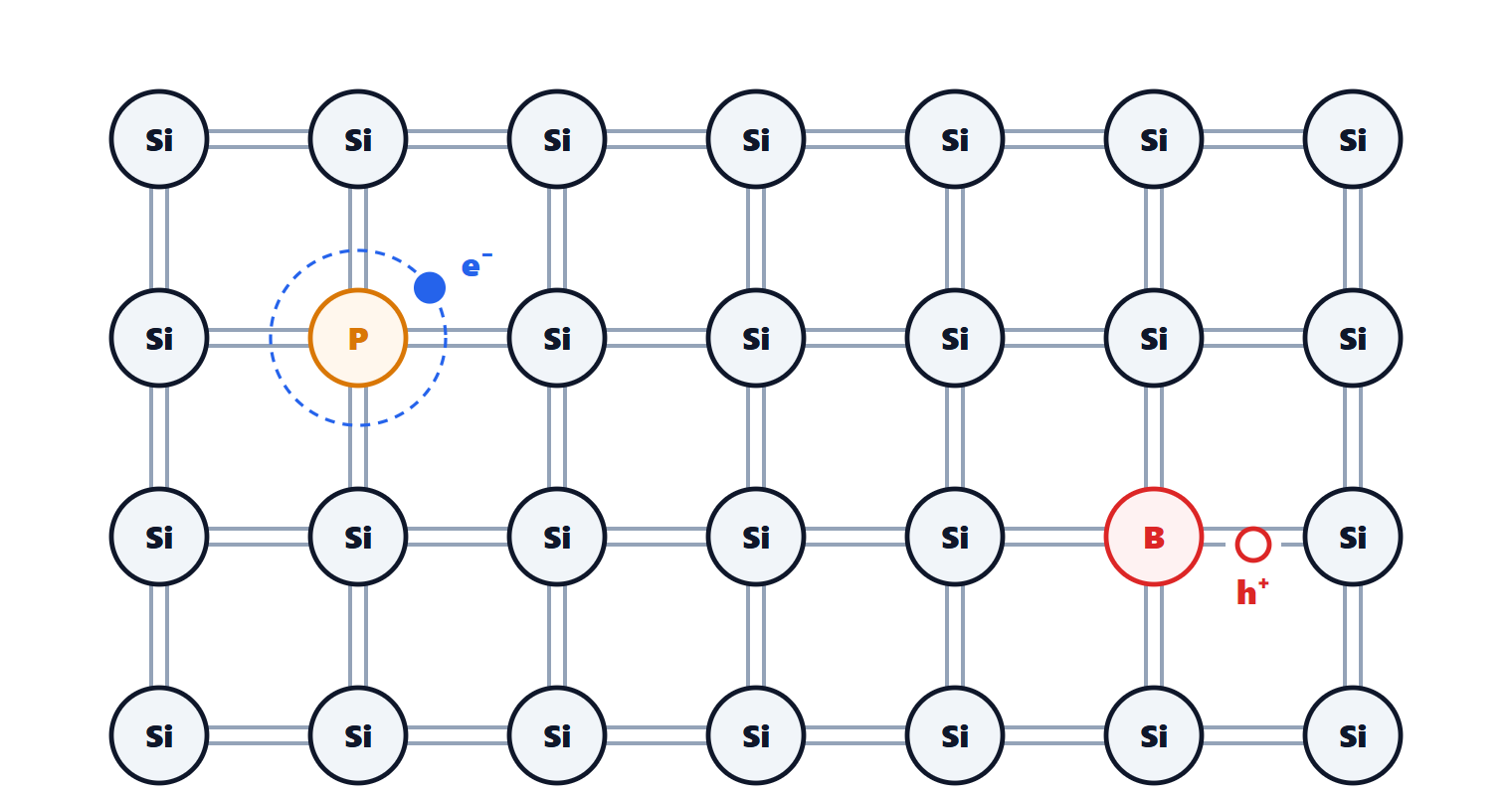
Tiny concentrations are enough: with  cm⁻³, one phosphorus atom every five million silicon atoms, free electrons become a million times more numerous than in pure silicon.
The mass action law
Theorem. At thermal equilibrium, in a non-degenerate semiconductor, doped or not,

Proof. With Boltzmann statistics, the concentrations depend on the distance of the Fermi level  from the bands:

Multiplying, cancels:  , which depends only on the material and the temperature. In the intrinsic case , so the constant equals
 . ∎
The physical meaning: electrons and holes are generated in pairs by thermal agitation and recombine when they meet, and the rate of encounters is proportional to the product  . At equilibrium generation and recombination balance.
Majority and minority carriers
In an n-type material with  , all donors are ionised, so
 , and from the mass action law

Example. With cm⁻³:  cm⁻³ and
 cm⁻³. Electrons are the majority carriers, holes the minority carriers, twelve orders of magnitude fewer. By adding electrons, doping increases recombination and so decreases the holes.
In p-type the opposite holds:  ,
 . If a material contains both donors and acceptors, the difference is what counts: this is how layers of different type are built on top of each other in the same crystal.
Temperature
Doping controls the majority carriers only as long as  stays much smaller than the doping. Since grows exponentially with
 (it roughly doubles every 9 °C in silicon), above a certain temperature the material behaves as intrinsic again and devices stop working. In silicon the practical limit is around 150 to 200 °C; wide-gap semiconductors such as silicon carbide (3.3 eV) and gallium nitride (3.4 eV) withstand much higher temperatures, which is why they are used in the power electronics of electric cars and compact chargers.