Oscillators in depth: designing a Colpitts, the crystal and Leeson's phase noise
Step-by-step design of a Colpitts oscillator, the Clapp variant, the electrical model of the crystal with the series and parallel resonances proved, the three regions of phase noise in Leeson's model.
https://www.electronics-engineering.com/en/oscillators-in-depth-colpitts-design-crystal-leeson/
This page goes deeper into the lesson on oscillators: it designs a Colpitts step by step, from the capacitance to the bias current, presents the Clapp variant, derives the two resonances of the crystal from its electrical model and explains where the three regions of phase noise in Leeson’s model come from.
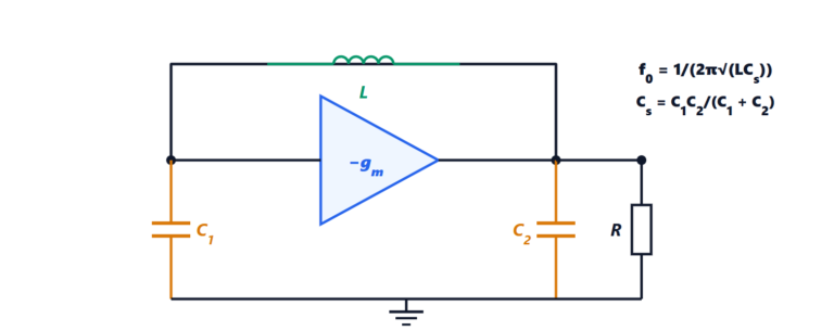
Designing a Colpitts step by step
The formulas of the proof are enough for a complete design. Goal: a 10 MHz oscillator with a 2.2 µH inductor of quality factor  , driving a 2 kΩ load.
Step 1: the series capacitance. From  :

With  we have
 , so
 pF (in practice 220 pF plus the capacitance of the transistor and of the circuit board).
Step 2: the loss resistance. An inductor with quality factor  is equivalent, near resonance, to an ideal inductor with the resistance
 kΩ in parallel. In parallel with the 2 kΩ load it gives
 kΩ: this is the
 of the formula.
Step 3: the required gain. The start-up condition requires

With a margin of 4,  mS. For a bipolar transistor
 , so
 µA.
Step 4: the corrections. The proof assumed that the amplifier input draws no current. A bipolar transistor instead has an input resistance  (about 40 kΩ with
 ), which adds to the losses: in practice a somewhat higher current is chosen, 0.2 to 1 mA, and start-up is checked in simulation or on the bench. Too much current, however, drives the transistor into heavy compression and increases the harmonics.
Estimating the amplitude. With a large margin the transistor works almost as a switch, and the fundamental component of the collector current approaches  . The output amplitude is therefore about
 : with
 mA and
 kΩ, about 1.7 V peak. This is the mechanism by which the oscillator regulates its own amplitude.
The Clapp variant
In the Colpitts the frequency depends on  and
 , to which the transistor capacitances add, and these change with temperature and bias. The Clapp adds a small capacitor
 in series with the inductor:

If  , the equivalent capacitance is almost and the frequency hardly depends on the transistor any more. The price is a lower loop gain, because attenuates the signal fed back to the input.
The crystal: electrical model and two resonances
A crystal is represented by the Butterworth-Van Dyke model: a series branch  ,
 ,
 (the mechanical vibration seen as a circuit) in parallel with the electrode capacitance
 .
Theorem. The crystal has a series and a parallel resonance:

Proof. Neglecting , the reactance of the series branch is  , zero for
 : this is the series resonance, where the crystal impedance is minimum. The series branch is in parallel with , whose reactance is
 ; the impedance of the parallel combination becomes infinite when the two reactances are equal and opposite, that is
 . Multiplying by
 :
 , which gives
 . Since
 , the expansion
 gives the approximate form. ∎
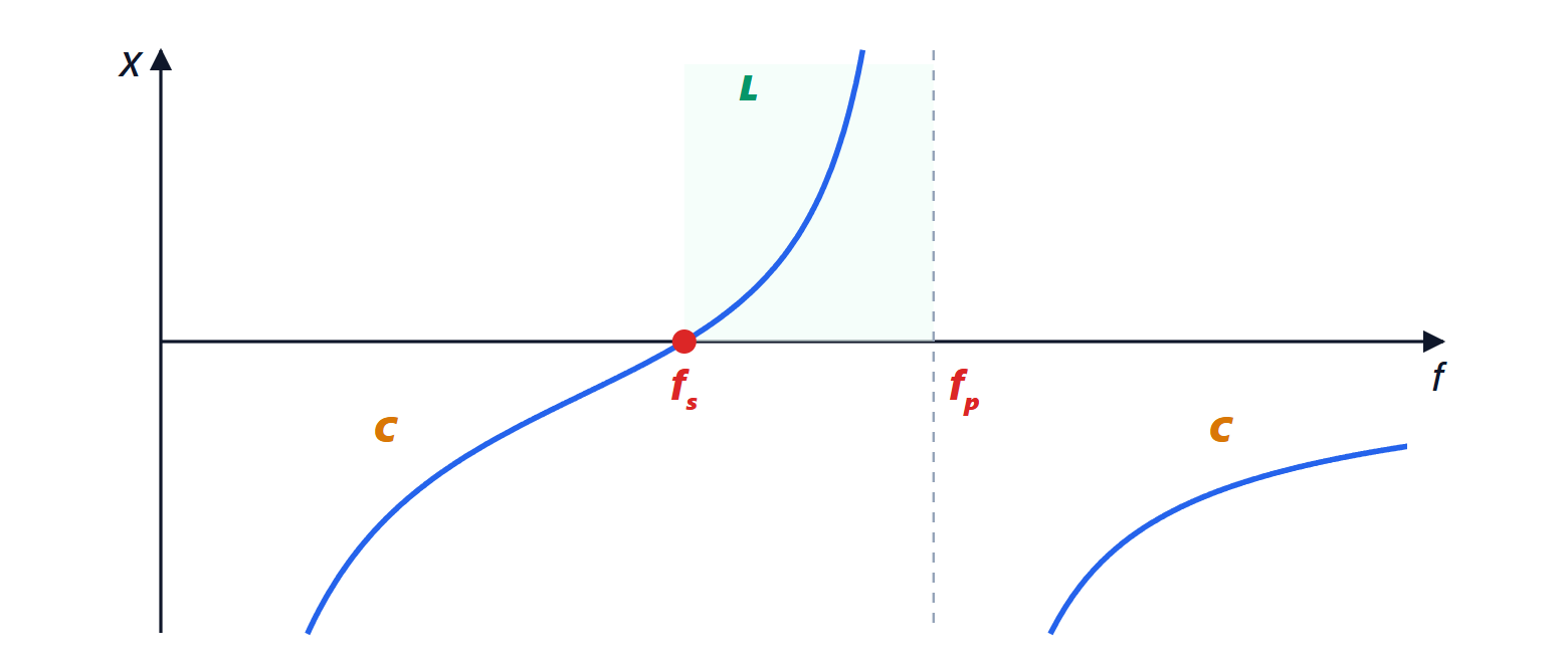
The band between  and is extremely narrow, and there the crystal behaves like an inductor that changes enormously with frequency. In a crystal Colpitts the crystal takes the place of
 : the circuit finds by itself the frequency, inside that band, that satisfies the phase condition, and small phase shifts move it very little. It is the extreme version of the link between
 and stability shown in the lesson.
Why phase noise has that shape
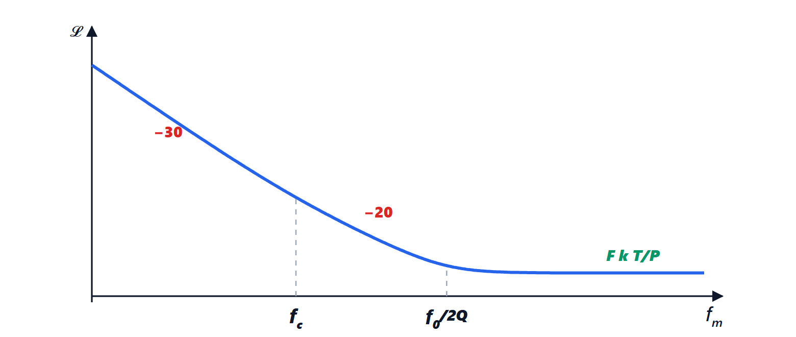
The plot of Leeson’s model has three regions, each with a simple explanation.
- Far from the carrier the noise is flat: it is the thermal noise of the amplifier,
 , divided by the signal power
 (the 2 accounts for the two sidebands).
- Inside the resonator bandwidth, for
 , the loop converts phase fluctuations into frequency fluctuations: a phase that fluctuates by
 shifts the frequency by
 , as proved in the lesson. Frequency noise, integrated, becomes phase noise with a factor
 in amplitude, that is
 in power: a slope of −20 dB per decade.
- Very close to the carrier the
 (flicker) noise of the transistor is added, which below the corner frequency
 multiplies everything by
 : the slope becomes −30 dB per decade.

Common mistakes
- Adding and : as seen from the inductor the two capacitors are in series, and the frequency is computed with
 .
- Forgetting the gain margin: with
 exactly equal to
 the circuit does not start, because tolerances and temperature push it below the threshold.
- Neglecting the loading of the transistor input:
 and the base-emitter capacitance become part of the network and change both the start-up condition and the frequency.
- Confusing and of the crystal: in a parallel oscillator the actual frequency depends on the load capacitance given in the datasheet, and with a different capacitance the crystal works off frequency.
- Reading dBc/Hz as a total power: to know how much noise enters a channel one must add
 of its bandwidth.
Exercises on the topic, from the frequency of a Colpitts to reciprocal mixing in a receiver, are on the exercise page linked at the top.