The History of the Transistor
The transistor is a SOLID-STATE device made of SEMICONDUCTORS. Its operation is based on that of the P-N JUNCTION, which was discovered by chance by RUSSELL…
https://www.electronics-engineering.com/en/the-history-of-the-transistor/

The transistor is a SOLID-STATE device made of SEMICONDUCTORS. Its operation is based on that of the P-N JUNCTION, which was discovered by chance by RUSSELL OHL on 23 FEBRUARY 1939.
Replica of the first transistor
The transistor is a solid-state device made of semiconductors. Its operation is based on that of the P-N junction, which was discovered by chance by Russell Ohl on 23 February 1939, while examining the difference in conductivity between the two sides of a cracked crystal of semiconductor silicon.
The first transistor was built with point contacts and was of the order of a centimetre in size. It was built in 1947 by Walter Brattain, who together with William Shockley and John Bardeen received the Nobel Prize in Physics in 1956, with the citation: “for their researches on semiconductors and their discovery of the transistor effect”.
Transistors are used in electronics mainly as amplifiers of electrical signals or as electronic switches controlled by electrical signals, and they have almost completely replaced thermionic valves.
The first type of transistor to be tested and then produced was the bipolar transistor or BJT, in which both electrons and holes contribute to the flow of current. Later other types of transistor were created, in which current flows thanks to only one type of charge carrier (either electrons or holes), called FETs, an acronym for Field Effect Transistor. Both FETs and BJTs have, over time, given rise to many different types of transistor, used for the most varied purposes.
Bipolar transistor (BJT)
In a BJT (bipolar junction transistor) an electric current is sent into the base (B) and modulates (controls) the current that flows between the other two terminals, known as the emitter (E) and the collector (C).
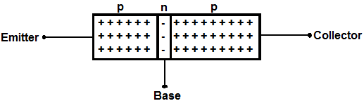
To do this, the transistor exploits the proximity of two opposite P-N junctions: when the base-emitter junction is forward biased, the charge carriers (electrons and holes) that pass through it diffuse towards the nearby collector-base junction, where they are largely captured by the electric field inside the junction itself, which in this way carries current even though it is reverse biased. The greater the fraction of current captured by the collector junction, the better the transistor: in an ideal, perfect transistor, all the current entering from the emitter would be diverted to the collector without ever reaching the base contact. In practice, in a normal general-purpose transistor the current leaving the collector is 98-99% of that entering the emitter, and only 1-2% of it leaves through the base. The ratio between collector current and base current is called the β (beta) of the transistor, and it is one of the fundamental parameters of this device.
The order of the junctions is not important: you can use either a pair of P-N and N-P junctions (obtaining a P-N-P transistor) or two N-P and P-N junctions (obtaining an N-P-N transistor, complementary to the first): a transistor and its complement work in an almost identical way, but the voltages across them must have their polarity reversed (from positive to negative and vice versa).
FET transistor
In a FET (field-effect transistor) the three terminals are called gate G, source S and drain D respectively, and the transistor effect is obtained through the electric field induced by the voltage applied to the gate terminal, which repels the charge carriers of the silicon in the channel between source and gate, changing its electrical resistance: the larger the voltage between gate and source, the wider the non-conducting depleted region, free of carriers, becomes, and the more the electrical resistance between source and drain grows. Compared with bipolar transistors, FETs have the advantage that the control terminal (gate) is insulated and no current flows through it; the disadvantage, instead, is that a FET cannot supply much output current: in general circuits with FETs have a high output impedance, that is they deliver very weak currents.
FETs too, like bipolar transistors, can be made in two complementary versions, with a P channel flanked by N regions or an N channel flanked by P regions (like the one in the figure at the side); as with bipolar transistors the operation is identical, but with reversed polarities.
MOSFET transistor
MOSFET transistors are FETs in which the voltage applied to the gate not only creates a depleted zone free of carriers, but, if it grows beyond a voltage called the “threshold”, causes an inversion of the population in the silicon next to the oxide layer: in the figure at the side, the two regions of the source and drain terminals are made of P silicon, and are in electrical communication through the “P channel” created by inversion in the N layer that separates them, thanks to the voltage applied to the gate across the oxide surface barrier. Here too the regions can be swapped: the figure shows a p-channel MOSFET (p-MOS); its complement (n-MOS) is obtained with a P substrate into which the N source and drain regions are inserted. As with bipolar transistors, the operation of p-MOS and n-MOS devices is also (almost) identical, but with reversed polarities.
While BJTs are mainly used, for their high gain, as amplifiers in analog electronics, MOSFETs are widely used in digital electronics, above all because of their very simple structure, which makes them easy to build and cheap to use in integrated circuits: a further advantage is their low power consumption, which means fewer heat-dissipation problems, while the main disadvantage is that they are slower to change state than bipolar transistors. Modern MOSFET integrated circuits (microprocessors, DSPs, microcontrollers, etc.) all use CMOS (complementary MOS) technology, in which paired p-MOS and n-MOS transistors are used, or its evolution BiCMOS.
Other types of transistor
As technology has evolved, other types of transistor have also been created, with different characteristics or suited to particular uses: for example the unijunction transistor or UJT is a pulse generator and can neither amplify nor switch. IGBTs (Insulated Gate Bipolar Transistors), on the other hand, are hybrid devices between bipolar transistors and MOSFETs, suited to handling large currents. There are also transistors developed for research applications; these are developed to achieve extreme performance such as high currents or high operating frequencies. In June 2006 a silicon-germanium transistor reached a switching frequency of 500 GHz in the laboratory.
Transistor radios
In everyday language the small battery-powered portable AM/FM radios are also called transistors; they were the first application of these devices to reach the mass market, in the 1950s.


Biasing the NPN transistor
Objective: Determine the values of the resistors RB and RC that allow an NPN transistor to operate in the active region.
Data:
VCC (supply voltage): 10 V
IC (desired collector current): 4 mA
VCE (desired collector-emitter voltage): 5 V
Beta (current gain of the transistor): 80
Principles:
Active region: The transistor operates as an amplifier when it is biased in the active region. In this region, the base-emitter junction is forward biased and the collector-base junction is reverse biased.
Kirchhoff’s laws:
The sum of the voltages around a loop is zero.
The sum of the currents at a node is zero.
Calculation of the resistances:
RB (base resistor): Controls the base current (IB).
Using Kirchhoff’s law for the input loop: VCC – RB * IB – VBE = 0.
VBE is the base-emitter voltage, typically 0.7 V for a silicon transistor in the active region.
IB = IC / Beta.
Solving for RB: RB = (VCC – VBE) / IB = Beta * (VCC – VBE) / IC = 186 kΩ.
RC (collector resistor): Determines the voltage drop across the collector-emitter junction (VCE).
Using Kirchhoff’s law for the output loop: VCC – RC * IC – VCE = 0.
Solving for RC: RC = (VCC – VCE) / IC = 1.25 kΩ.
Conclusion:
By selecting RB = 186 kΩ and RC = 1.25 kΩ, the NPN transistor will operate in the active region with the desired collector current and collector-emitter voltage.





Sono l'autore di questa pagina su «La Storia del Transistor». Se qualcosa non è chiaro, se vi serve un esempio in più o volete approfondire un punto, scrivetelo qui sotto nei commenti: rispondo personalmente. Se la pagina vi è stata utile, lasciate un voto con le stelle in cima all'articolo.