The pn junction: depletion region, field and built-in potential
Formation of the depletion region, built-in potential with proof, depletion width from Poisson's equation, biasing, junction capacitance and solar cells.
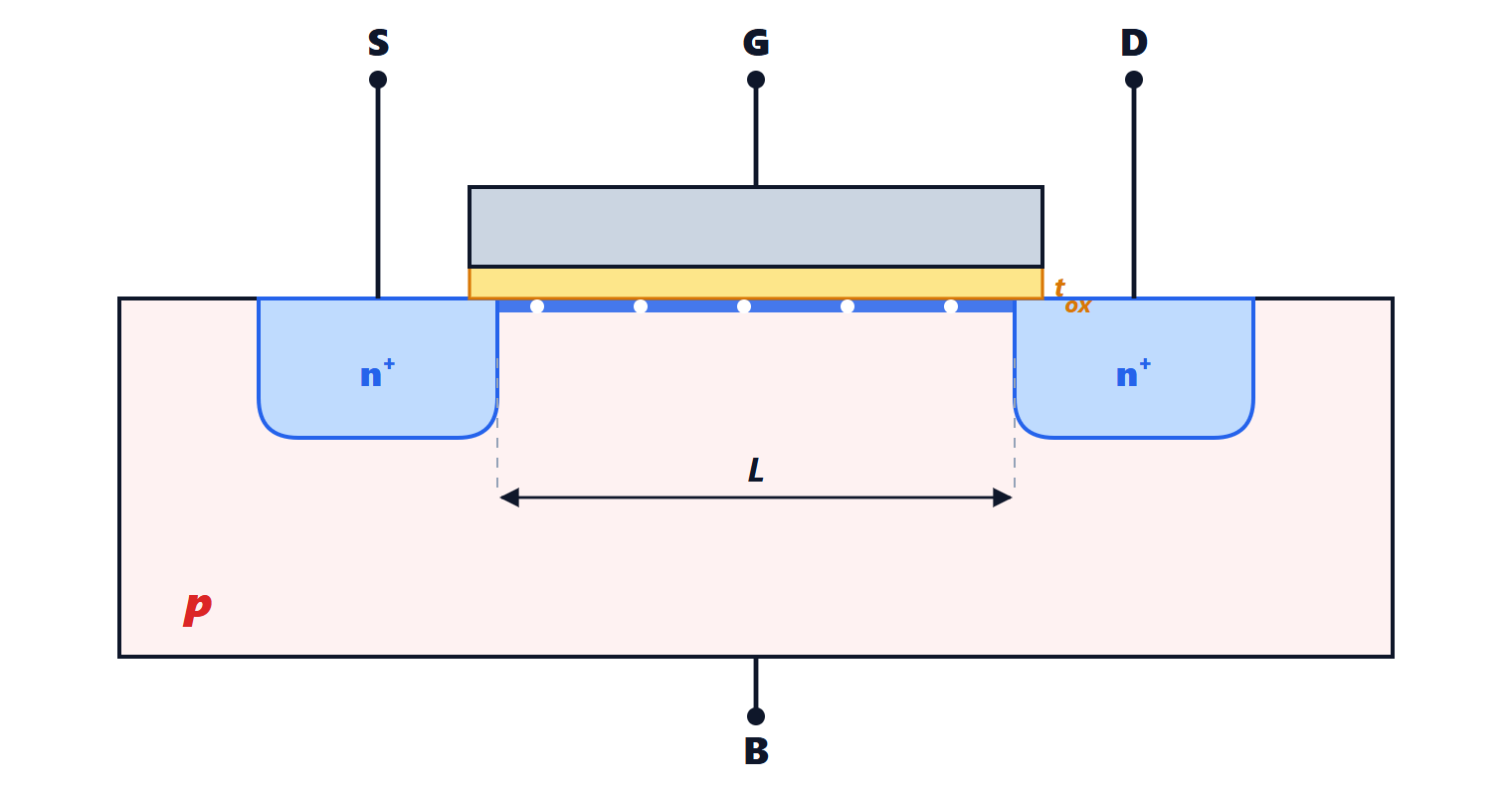
Bringing a p-type region and an n-type region into contact, in the same crystal, gives the pn junction, the building block of almost every device: diodes, LEDs, solar cells, bipolar transistors, and MOSFETs too, whose source and drain terminals are junctions. In this lesson we look at what happens at equilibrium: the depletion region, the built-in field, the contact potential and how they change when a voltage is applied.
What happens at contact
On the p side holes are plentiful, on the n side there are almost none; for electrons it is the reverse. As soon as the two regions are in contact, holes diffuse towards n and electrons towards p, where they recombine with the majority carriers.
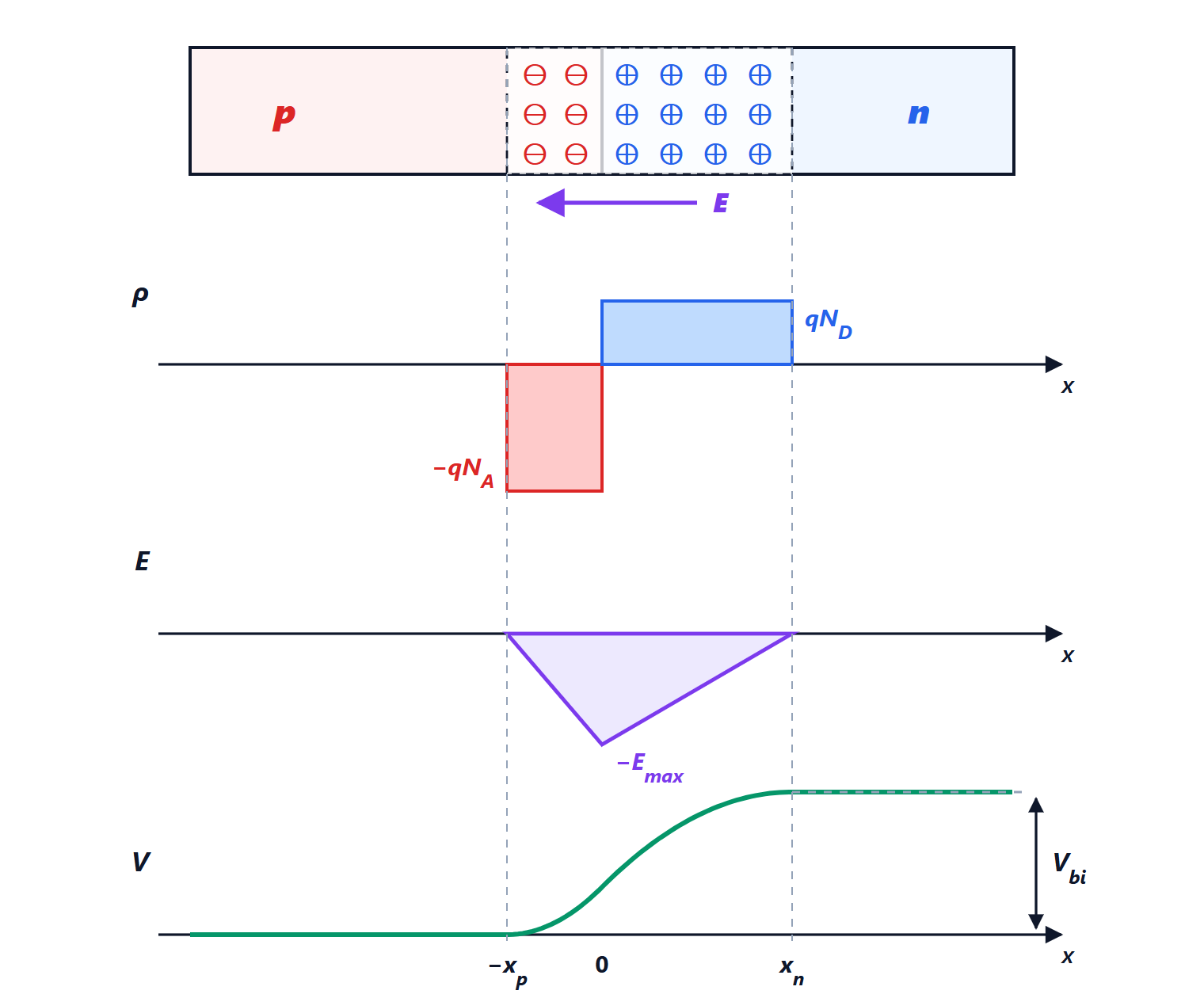
As they leave, the carriers uncover the fixed dopant ions: negative acceptors on the p side, positive donors on the n side. So a depletion region (or space-charge region) forms across the junction, almost free of mobile carriers, with negative charge on one side and positive on the other. This charge creates an electric field pointing from n to p, which opposes diffusion: equilibrium is reached when the drift current produced by the field exactly balances the diffusion current, for electrons and for holes separately.
The built-in potential
Theorem. Across the depletion region there is a potential difference
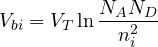
Proof. At equilibrium the total electron current is zero at every point, and as in the proof of the Einstein relation it follows that the concentration obeys Boltzmann’s law:  . Comparing the two ends, far from the junction,
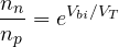
with  (majority carriers on the n side) and
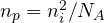 (minority carriers on the p side). Taking the logarithm gives the formula. ∎
Example. With  cm⁻³ and
 cm⁻³:
 V. The built-in potential cannot be measured with a voltmeter: at the metal contacts other potential differences arise that cancel it exactly, otherwise a diode at rest would deliver energy.
The width of the depletion region
We use the depletion approximation: in the depletion region, from  to
 , there are no mobile carriers; outside it the charge is zero.
Neutrality. The total charge must be zero, so  : the region extends mostly into the more lightly doped side.
Field. From Poisson’s equation  , with piecewise constant
 , the field is piecewise linear: it starts from zero at , reaches its largest magnitude at the junction and returns to zero at :

Potential. The potential difference is the area of the field triangle:  , with
 . Combining the three relations:
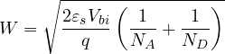
Example. With the doping above and  :
 µm, of which 0.30 µm on the n side and only 0.03 µm on the p side, ten times more heavily doped. The peak field is about
 V/cm: less than a volt across a third of a micrometre gives a very strong field.
The biased junction
When an external voltage  is applied (positive if the p side is more positive), almost all of it drops across the depletion region, because that is where carriers are missing and the resistance is very high. The barrier becomes
 , and in the formulas you simply substitute:

- Reverse bias (
 ): the barrier grows, the depletion region widens and diffusion is blocked. Only a tiny minority-carrier current flows. With
 V the region in the example widens to about 1.24 µm.
- Forward bias (
 ): the barrier is lowered, the region narrows and diffusion resumes exponentially. This is the behaviour of the diode, which we study in the next lesson.
Junction capacitance
The charges on the two sides of the depletion region are like the plates of a capacitor at distance  :
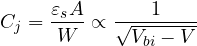
The capacitance decreases as the reverse voltage increases. It is a drawback in fast circuits, because it must be charged and discharged at every switching event, but it becomes an asset in varicap diodes: voltage-controlled capacitors used to tune oscillators and receivers with no moving parts.
The field as a charge separator
If an electron-hole pair is generated in the depletion region, or within a diffusion length of it, for instance by a photon, the built-in field immediately separates the two charges: the electron goes towards n, the hole towards p. This is the principle of photodiodes and solar cells: the junction turns light into current with no external supply. In solar cells the aim is a wide active region and slow recombination, because every pair that recombines before being separated is lost energy.