Radio-frequency amplifiers: stability, gain and noise
The Rollett factor with an example, maximum unilateral gain proved, the gain-noise trade-off in LNAs, inductive degeneration, biasing.
The first block of every receiver is a low-noise amplifier (LNA), and its design sets the sensitivity of the whole radio (Electrical Communications lesson on receiver noise). At radio frequency an amplifier is designed with the transistor’s S-parameters: one chooses what to present at its input and output with the matching networks. In this lesson we look at stability with the Rollett factor and a numerical example, maximum gain with its proof in the unilateral case, the trade-off between gain and noise, and biasing.
The structure
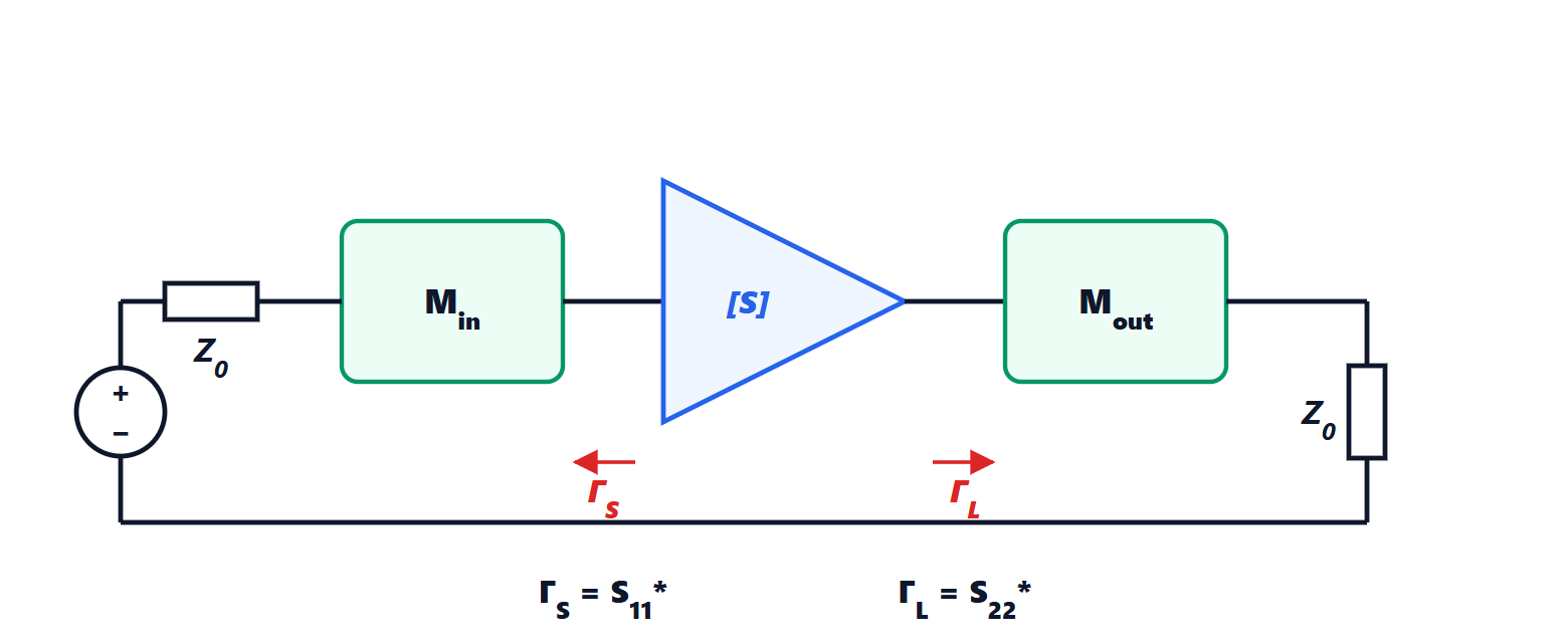
The design consists in choosing the reflection coefficients  and
 that the networks present to the transistor, and then in realising the networks (lesson on matching).
Stability
A transistor always has some internal feedback ( ): with certain source and load impedances the reflection coefficient seen at one port exceeds 1 in magnitude, the port gives back more power than it receives and the circuit oscillates. First of all stability must be checked at all frequencies, even far from the operating band, where the transistor still has gain.
A two-port is unconditionally stable (stable with any passive source and load) if and only if

(Rollett criterion).
Example. A transistor with, for simplicity, real parameters  ,
 ,
 ,
 :
 , and
 . Unconditionally stable. With
 we would get
 : borderline. When
 the transistor is stabilised with resistors in series or in parallel at the input or output (which cost gain and, at the input, noise), or and are chosen far from the unstable regions, represented on the Smith chart by stability circles.
Maximum gain
If  is negligible (unilateral transistor), input and output do not affect each other and the transducer gain (power in the load divided by the power available from the source) splits into three factors:

Theorem. The maximum unilateral gain, obtained with  and
 , is

Proof. The input factor is the ratio between the power entering the transistor and that available from the source through the network; it is maximum when the network achieves conjugate matching, i.e. when the reflection coefficient seen by the transistor is the conjugate of its own, (lesson on matching). Substituting, the denominator becomes  and the factor reduces to
 . The same holds for the output. ∎
Example. With the previous transistor:  (12.0 dB),
 (1.9 dB),
 (1.2 dB): about 15.2 dB in total. The matching networks add 3.2 dB to the gain the transistor would have between two 50 Ω loads, recovering the power that would otherwise be reflected. When is not negligible bilateral formulas are used, and the maximum exists only if the transistor is unconditionally stable.
Gain and noise
The noise added by the transistor depends on the source impedance it sees, and there is a  that minimises the noise figure,
 . In general
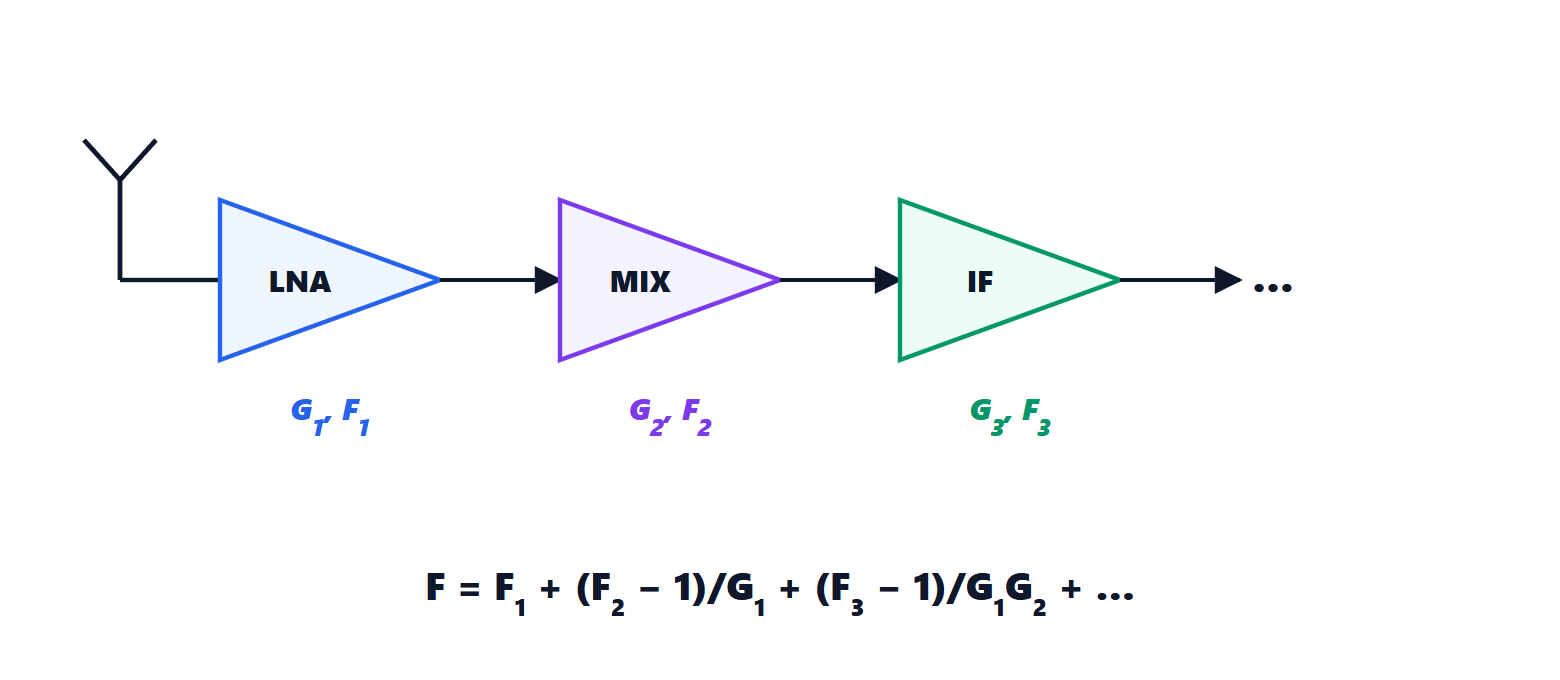
 : maximum gain and minimum noise cannot be had together. For an LNA is chosen close to , accepting a slightly mismatched input and somewhat lower gain. On the Smith chart the loci of equal noise figure and equal gain are circles, and the designer chooses a compromise point. By Friis’s formula, if the first stage has enough gain the noise of the following stages matters little, so the LNA’s gain serves mainly to “protect” the rest of the chain.
Techniques such as inductive emitter (or source) degeneration bring the two conditions closer: an inductor in series with the emitter creates a real part at the input without adding noise, and brings the power match close to the noise match.
Biasing
The transistor must be supplied with DC without disturbing the signal: RF chokes are used, which let DC through but present a high impedance at radio frequency, and blocking capacitors separate DC between stages. The combination is called a bias tee. Bias networks must also be stable at low frequency, where the transistor has very high gain: many RF amplifier oscillations arise there, at a few megahertz, far from the operating band.